HEF4071BP 데이터 시트보기 (PDF) - NXP Semiconductors.
부품명
상세내역
일치하는 목록
HEF4071BP Datasheet PDF : 11 Pages
| |||
NXP Semiconductors
HEF4071B
Quad 2-input OR gate
10. Dynamic characteristics
Table 7. Dynamic characteristics
Tamb = 25 °C; waveforms see Figure 4; test circuit see Figure 5; unless otherwise specified. [1]
Symbol Parameter
Conditions VDD
Extrapolation formula Min Typ
tPHL
HIGH to LOW
nA or nB to nY 5 V
propagation delay
10 V
28 + 0.55 × CL
15 + 0.23 × CL
-
55
-
25
15 V
12 + 0.16 × CL
-
20
tPLH
LOW to HIGH
nA or nB to nY 5 V
propagation delay
10 V
18 + 0.55 × CL
9 + 0.23 × CL
-
45
-
20
15 V
7 + 0.16 × CL
-
15
tt
transition time
5 V [2] 10 + 1.0 × CL
-
60
10 V
9 + 0.42 × CL
-
30
15 V
6 + 0.28 × CL
-
20
Max Unit
115 ns
50 ns
35 ns
90 ns
45 ns
30 ns
120 ns
60 ns
40 ns
[1] The typical value of the propagation delay and output transition time can be calculated with the extrapolation formula (CL in pF).
[2] tt is the same as tTHL and tTLH.
Table 8. Dynamic power dissipation
VSS = 0 V; tr = tf ≤ 20 ns; Tamb = 25 °C.
Symbol Parameter
VDD Typical formula
where:
PD
dynamic power dissipation 5 V PD = 1150 × fi + Σ(fo × CL) × VDD2 (µW) fi = input frequency in MHz;
10 V PD = 4800 × fi + Σ(fo × CL) × VDD2 (µW) fo = output frequency in MHz;
15 V PD = 19700 × fi + Σ(fo × CL) × VDD2 (µW) CL = output load capacitance in pF;
Σ(fo × CL) = sum of the outputs;
VDD = supply voltage in V.
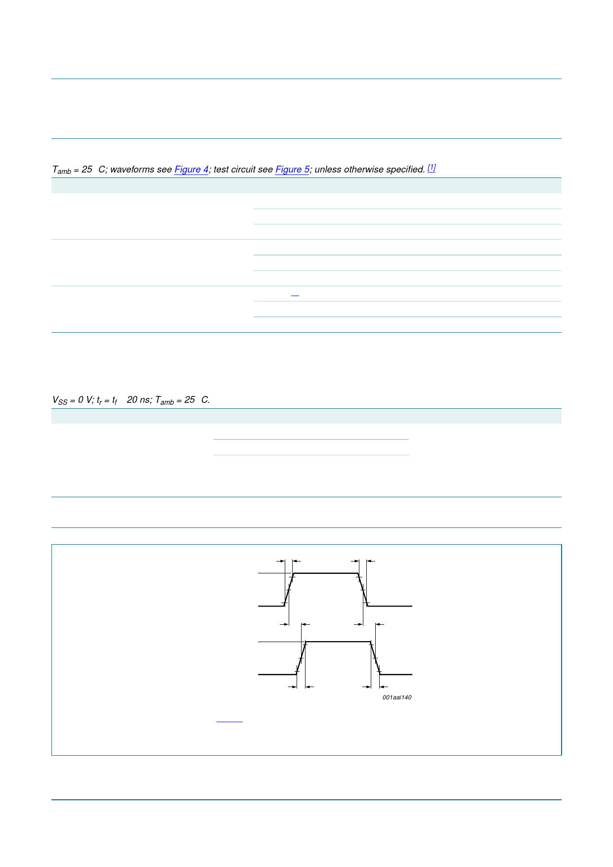
11. Waveforms
VI
nA, nB input
10 %
0V
tr
90 %
VM
tPLH
VOH
nY output
VOL
10 %
90 %
VM
tTLH
tf
tPHL
tTHL
001aai140
Fig 4.
Measurement points are given in Table 9.
Logic levels: VOL and VOH are typical output voltage levels that occur with the output load.
Input to output propagation delay and output transition times
HEF4071B_4
Product data sheet
Rev. 04 — 28 November 2008
© NXP B.V. 2008. All rights reserved.
5 of 11
Share Link: 