CS8271 데이터 시트보기 (PDF) - Cherry semiconductor
부품명
상세내역
일치하는 목록
CS8271 Datasheet PDF : 6 Pages
| |||
Application Notes: continued
Step 6: Test the load transient response by switching in
various loads at several frequencies to simulate its real
work environment. Vary the ESR to reduce ringing.
Step 7: Remove the unit from the environmental chamber
and heat the IC with a heat gun. Vary the load current as
instructed in step 5 to test for any oscillations.
Once the minimum capacitor value with the maximum
ESR is found, a safety factor should be added to allow for
the tolerance of the capacitor and any variations in regula-
tor performance. Most good quality aluminum electrolytic
capacitors have a tolerance of ±20% so the minimum value
found should be increased by at least 50% to allow for this
tolerance plus the variation which will occur at low tem-
peratures. The ESR of the capacitor should be less than
50% of the maximum allowable ESR found in step 3 above.
Capacitance on the Adjust pin combined with the feed-
back resistors R1 and R2 can affect loop stability and
should also be considered. The CS8271 internal circuitry
produces about 5pF to Ground on the Adjust pin. This
capacitance, plus any additional external capacitance on
the Adjust pin will create a pole when combined with the
resistive feedback network. The effect can be significant
when using large values for the feedback resistors to mini-
mize quiescent current.
A capacitor connected from the Adjust pin to Ground pro-
vides additional means to compensate the regulator by
creating a pole. Alternately, a capacitor can be connected
from the Adjust pin to VOUT to create a zero.
where
VIN(max) is the maximum input voltage,
VOUT(min) is the minimum output voltage,
IOUT(max) is the maximum output current, for the applica-
tion
IQ is the quiescent current the regulator consumes at
IOUT(max).
IIN
VIN
Smart
Regulator
}Control
Features
IQ
IOUT
VOUT
Figure 4: Single output regulator with key performance parameters
labeled.
Once the value of PD(max) is known, the maximum permis-
sible value of RQJA can be calculated:
RQJA =
150¡C - TA
PD
(2)
Calculating Power Dissipation
in a Single Output Linear Regulator
The maximum power dissipation for a single output regu-
lator (Figure 4) is
PD(max)={VIN(max)ÐVOUT(min)}IOUT(max)+VIN(max)IQ
(1)
The value of RQJA can then be compared with those in
the package section of the data sheet. Those packages with
RQJA's less than the calculated value in equation 2 will keep
the die temperature below 150¡C.
In some cases, none of the packages will be sufficient to
dissipate the heat generated by the IC, and an external
heatsink will be required.
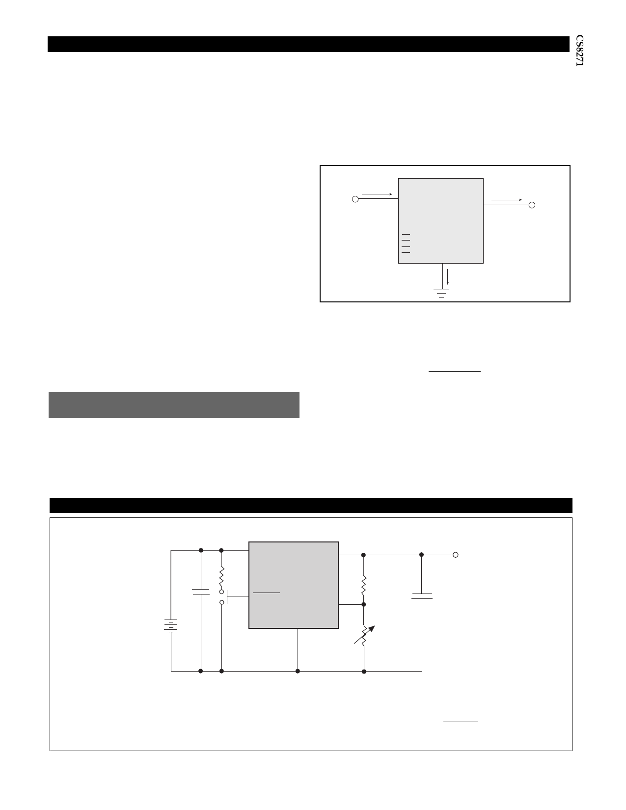
Application Diagram
C1*
0.1mF
VIN
VOUT
CS8271
ENABLE
Adj
Gnd
R1
Vref
R2
VOUT
C2**
10mF
C1* Required if regulator is away from power supply filter.
C2** Required for output stability.
5
( ) VOUT = Vref x
R1 + R2
R2
+ IAdj x R1
Share Link: 