CS8271 데이터 시트보기 (PDF) - Cherry semiconductor
부품명
상세내역
일치하는 목록
CS8271 Datasheet PDF : 6 Pages
| |||
Electrical Characteristics: VOUT + 1V ² VIN ² 30V, 5V ² VOUT ² 12V, IOUT = 10mA, -40¡ ² TA ² 125¡, -40¡ ² TJ ² 150¡,
VENABLE = 0V; unless otherwise specified.
PARAMETER
TEST CONDITIONS
MIN
TYP
MAX
UNIT
s ENABLE
Enable Threshold
1.15
2.0
2.6
V
Enable Input Current
VENABLE = 2.6V
VENABLE = 5V
10
20
µA
35
50
µA
s Adjustment Pin
Reference Voltage
Adjustment Pin Current
R1: Feedback resistor between VOUT and Adjust, R2: Adjust resistor to ground.
100µA ² IOU T² 100mA
IAdj =
VREF
R2
-
(VOUT - VREF)
R1
1.246
1.272
1.297
V
20
500
nA
Note 1: Guaranteed by design, not 100% tested in production.
PACKAGE PIN #
8L SOIC & PDIP
1
2
3, 6, 7
4
5
8
Package Pin Description
PIN SYMBOL
FUNCTION
VOUT
Gnd
NC
Adj
ENABLE
VIN
100mA output; adjustable from 5V to 12V.
Ground.
No Connection.
Resistor divider from VOUT to Adj, sets output voltage.
Logic level switch, when HIGH, regulator is in sleep mode.
Input voltage.
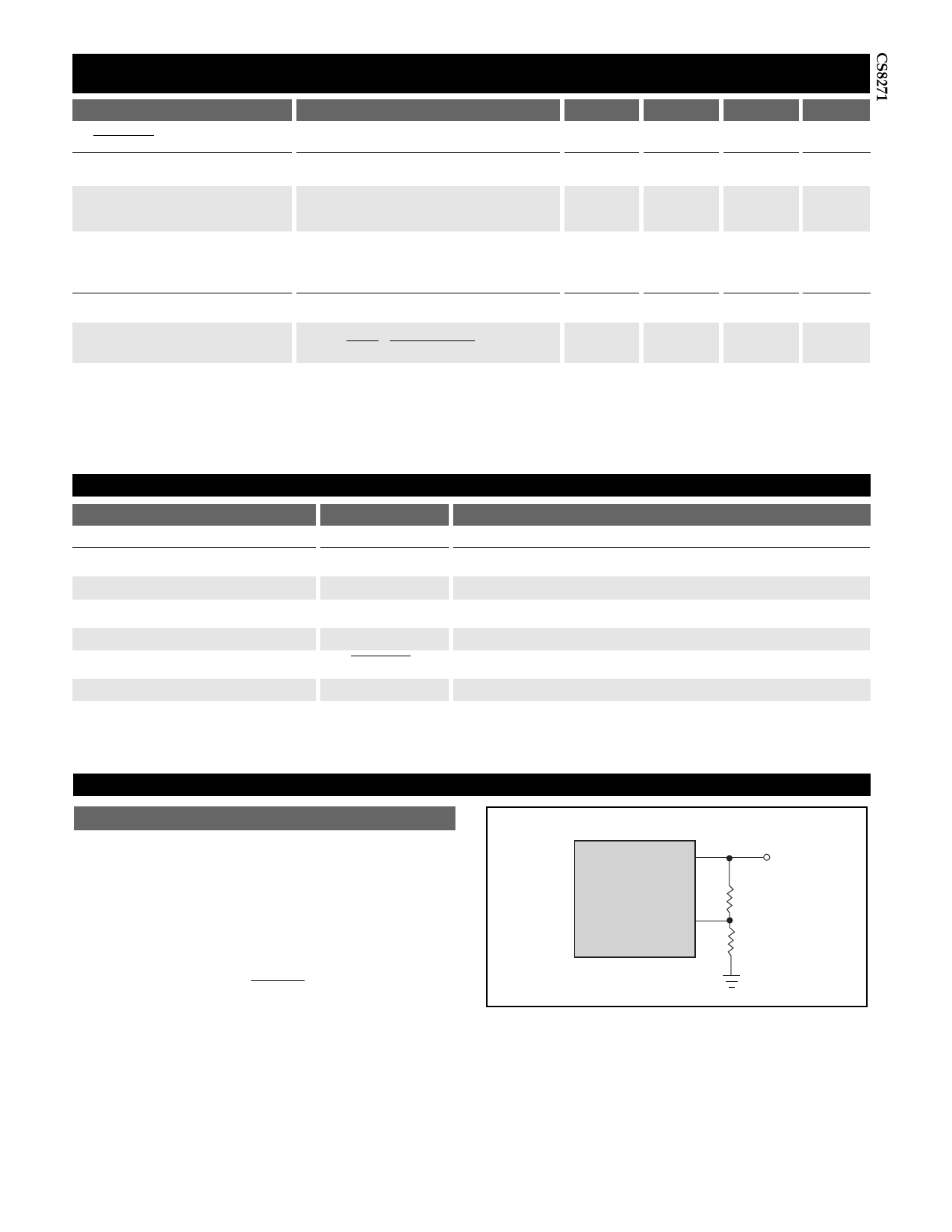
Circuit Description
Output Voltage Adjustment
The output voltage of the CS8271 is adjustable to any value
between the reference voltage on the Adj pin, (1.272V Typ.)
and the maximum input voltage minus the dropout voltage.
To adjust the output voltage, a pair of external resistors R1
and R2 are connected as shown in Figure 1.
The equation for the output voltage is
VOUT
CS8271
Adj
( ) VOUT = VREF x
R1 + R2
R2
+ IAdj x R1
where Vref is the typical reference voltage and IAdj is the
adjust pin bias current. This is usually 500nA maximum.
Figure 1: Output Voltage Adjustment.
VOUT
R1
VREF
R2
3
Share Link: 