CS8271 데이터 시트보기 (PDF) - Cherry semiconductor
부품명
상세내역
일치하는 목록
CS8271 Datasheet PDF : 6 Pages
| |||
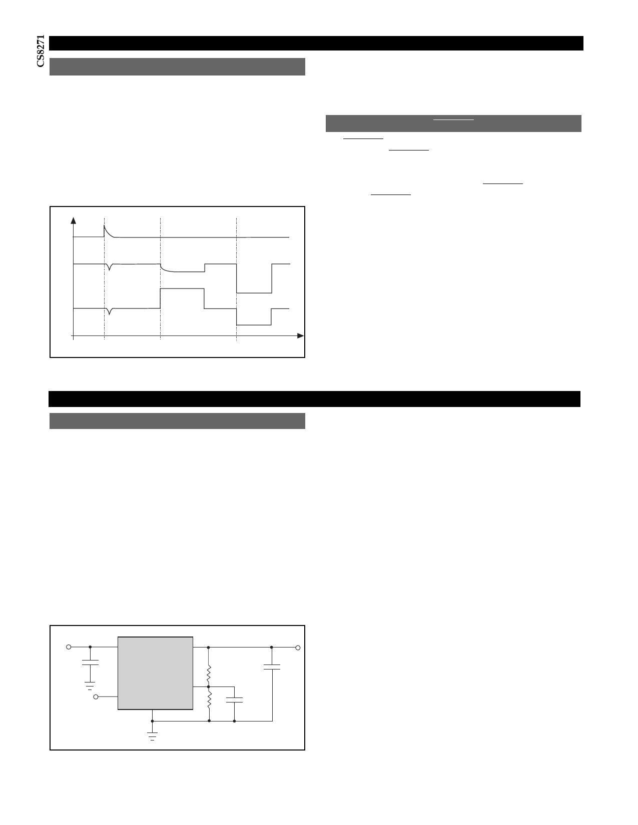
Circuit Description: continued
Output Stage Protection
The output stage is protected against overvoltage, short
circuit and thermal runaway conditions (Figure 2).
If the input voltage rises above 30V (e.g. load dump), the
output shuts down. This response protects the internal cir-
cuitry and enables the IC to survive unexpected voltage
transients up to 60V in magnitude.
Short circuit protection limits the amount of current the
output transistor can supply. In the case of a CS8271 under
a short circuit condition, the output transistor current is
limited to 100mA.
> 30V
Should the junction temperature of the power device exceed
180ûC (typ) the power transistor is turned off. Thermal shut-
down is an effective means to prevent die overheating since
the power transistor is the principle heat source in the IC.
ENABLE
The ENABLE switches the output transistor. When the
voltage on the ENABLE pin exceeds 2.0V typ, the output
pass transistor turns off, leaving a high impedance facing
the load. The IC will remain in Sleep mode, drawing only
20µA (typ), until the voltage on the ENABLE pin drops
below the ENABLE threshold.
VIN
VOUT
IOUT
Load
Dump
Short
Circuit
Thermal
Shutdown
Figure 2: Typical Circuit Waveforms for Output Stage Protection.
Application Notes
Selecting the Right Capacitor Value
The output compensation capacitor COUT, determines
three main characteristics of a linear regulator: start-up
delay, load transient response and loop stability.
The selection of a capacitor value and type should be
based on cost, availability, size and temperature con-
straints. A tantalum or aluminum electrolytic capacitor is
best, since a film or ceramic capacitor with almost zero
ESR, can cause instability. The aluminum electrolytic
capacitor is the least expensive solution, but, if the circuit
operates at low temperatures (-25¡C to -40¡C), both the
value and ESR of the capacitor will vary considerably. The
capacitor manufacturers data sheet usually provide this
information.
The value for the output compensation capacitor COUT
shown in Figure 3 should work for most applications, but it
is not necessarily the least expensive or the optimal solution.
VIN
CIN
0.1mF
VOUT
CS8271
Adj
ENABLE
RRST
COUT
10mF
RL
CAdj
(optional)
To determine an acceptable value for COUT for a particular
application, start with a tantalum capacitor of the recom-
mended value and work towards a less expensive alterna-
tive part.
Step 1: Place the completed circuit with a tantalum capac-
itor of the recommended value in an environmental cham-
ber at the lowest specified operating temperature. Monitor
the outputs on the oscilloscope. A decade box connected in
series with the capacitor will simulate the higher ESR of an
aluminum capacitor. (Leave the decade box outside the
chamber, the small resistance added by the longer leads is
negligible)
Step 2: With the input voltage at its maximum value,
increase the load current slowly from zero to full load
while observing the output for any oscillations. If no oscil-
lations are observed, the capacitor is large enough to
ensure a stable design under steady state conditions.
Step 3: Increase the ESR of the capacitor from zero using
the decade box and vary the load current until oscillations
appear. Record the values of load current and ESR that
cause the greatest oscillation. This represents the worst
case load conditions for the regulator at low temperature.
Step 4: Maintain the worst case load conditions set in step
3 and vary the input voltage until the oscillations increase.
This point represents the worst case input voltage condi-
tions.
Figure 3: Test and application circuit showing an output compensation
capacitor.
Step 5: If the capacitor is adequate, repeat steps 3 and 4
with the next smaller valued capacitor. (A smaller capaci-
tor will usually cost less and occupy less board space.) If
the capacitor oscillates within the range of expected oper-
ating conditions, repeat steps 3 and 4 with the next larger
standard capacitor value.
4
Share Link: 