PCK2014A 데이터 시트보기 (PDF) - Philips Electronics
부품명
상세내역
일치하는 목록
PCK2014A Datasheet PDF : 16 Pages
| |||
Philips Semiconductors
CK98 (100/133 MHz) spread spectrum
system clock generator
Product specification
PCK2014A
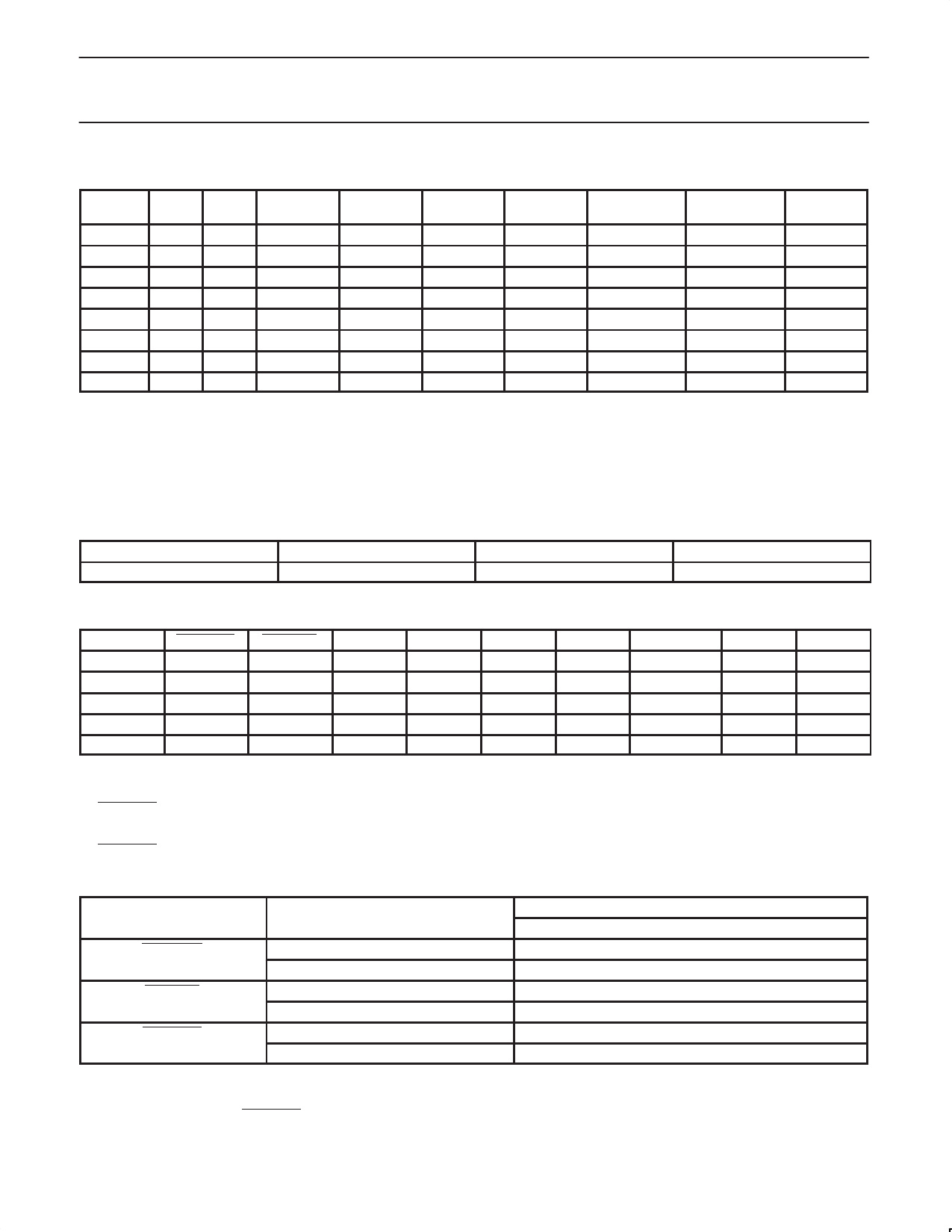
FUNCTION TABLE
SEL
133/100
SEL1
SEL0
CPU
3V66
PCI
48 MHz
REF
IOAPIC
0
0
0
HI-Z
HI-Z
HI-Z
HI-Z
HI-Z
HI-Z
0
0
1
100 MHz
66 MHz
33 MHz
48 MHz
14.318 MHz
16.67 MHz
0
1
0
100 MHz
66 MHz
33 MHz
HI-Z
14.318 MHz
16.67 MHz
0
1
1
100 MHz
66 MHz
33 MHz
48 MHz
14.318 MHz
16.67 MHz
1
0
0
TCLK/2
TCLK/4
TCLK/8
TCLK/2
TCLK
TCLK/16
1
0
1
133 MHz
66 MHz
33 MHz
48 MHz
14.318 MHz
16.67 MHz
1
1
0
133 MHz
66 MHz
33 MHz
HI-Z
14.318 MHz
16.67 MHz
1
1
1
133 MHz
66 MHz
33 MHz
48 MHz
14.318 MHz
16.67 MHz
NOTES:
1. Required for board level “bed-of-nails” testing.
2. Philips center spread mode.
3. 48 MHz PLL disabled to reduce component jitter. 48 MHz outputs to be held Hi-Z instead of driven to LOW state.
4. “Normal” mode of operation.
5. TCLK is a test clock over driven on the XTALIN input during test mode. TCLK mode is based on 133 MHz CPU select logic.
6. Required for DC output impedance verification.
7. Frequency accuracy of 48 MHz must be +167 PPM to match USB default.
8. Range of reference frequency allowed is MIN = 14.316 MHz, NOMINAL = 14.31818 MHz, MAX = 14.32 MHz
NOTES
1
2
3
4, 7, 8
5, 6
2
3
4, 7, 8
CLOCK OUTPUT
USBCLK7
TARGET FREQUENCY (MHz)
48.0
ACTUAL FREQUENCY (MHz)
48.008
PPM
167
CLOCK ENABLE CONFIGURATION
CPUSTOP PWRDWN PCISTOP CPUCLK
APIC
3V66
PCI
REF / 48 MHz OSC
VCOs
X
0
X
LOW
LOW
LOW
LOW
LOW
OFF
OFF
0
1
0
LOW
ON
LOW
LOW
ON
ON
ON
0
1
1
LOW
ON
LOW
ON
ON
ON
ON
1
1
0
ON
ON
ON
LOW
ON
ON
ON
1
1
1
ON
ON
ON
ON
ON
ON
ON
NOTES:
1. LOW means outputs held static LOW as per latency requirement below
2. ON means active.
3. PWRDWN pulled LOW, impacts all outputs including REF and 48 MHz outputs.
4. All 3V66 clocks as well as CPU clocks should stop cleanly when CPUSTOP is pulled LOW.
5. CPUDIV2, IOAPIC, REF, 48 MHz signals are not controlled by the CPUSTOP functionality and are enabled all in all conditions except when
PWRDWN is LOW.
POWER MANAGEMENT REQUIREMENTS
SIGNAL
SIGNAL STATE
LATENCY
NO. OF RISING EDGES OF FREE RUNNING PCICLK
CPUSTOP
0 (DISABLED)
1
1 (ENABLED)
1
PCISTOP
0 (DISABLED)
1
1 (ENABLED)
1
PWRDWN
1 (NORMAL OPERATION)
3 ms
0 (POWER DOWN)
2 MAX
NOTES:
1. Clock ON/OFF latency is defined as the number of rising edges of free running PCICLKs between the clock disable goes HIGH/LOW to the
first valid clock that comes out of the device.
2. Power up latency is when PWRDWN goes inactive (HIGH) to when the first valid clocks are driven from the device.
2001 Apr 02
5
Share Link: 