PCK2014A 데이터 시트보기 (PDF) - Philips Electronics
부품명
상세내역
일치하는 목록
PCK2014A Datasheet PDF : 16 Pages
| |||
Philips Semiconductors
CK98 (100/133 MHz) spread spectrum
system clock generator
Product specification
PCK2014A
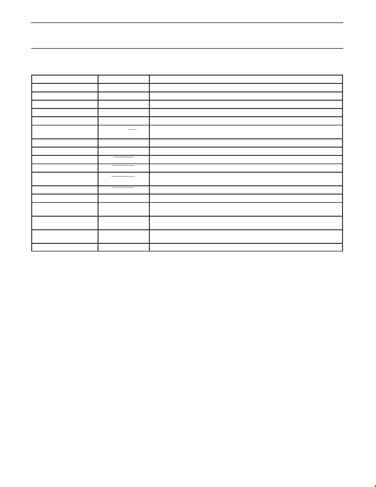
PIN DESCRIPTION
PIN NUMBER
SYMBOL
FUNCTION
2, 3
REF [0–1]
3.3 V 14.318 MHz clock output
5
XTAL_IN
14.318 MHz crystal input
6
XTAL_OUT
14.318 MHz crystal output
9, 11, 12, 14, 15, 18
PCI_[F, 1–5]
3.3 V PCI clock outputs, pin 9 is a free running PCI clock
25, 26
3V66 [0–1]
3.3 V fixed 66 MHz clock outputs
28
SEL133/100
Select input pin for enabling 133 MHz or 100 MHz CPU outputs.
H = 133 MHz, L = 100 MHz
30
48 MHz USB
3.3 V fixed 48 MHZ clock output
32, 33
SEL [0–1]
Logic select pins. TTL levels.
34
SPREAD
3.3 V LVTTL input. Enables spread spectrum mode when held LOW.
35
PWRDWN
3.3 V LVTTL input. Device enters powerdown mode when held LOW.
36
CPUSTOP
3.3 V LVTTL input. Stops all CPU clocks and 3V66 clocks when held LOW.
CPUDIV_2 output remains on all the time.
37
PCISTOP
3.3 V LVTTL input. Stops all PCI clocks except PCICLK_F when held LOW.
41, 42, 45, 46, 49, 50
CPUCLK [0–5] 2.5 V CPU output. 133 MHz or 100 MHz depending on state of input pin SEL133/100.
53, 54, 55
APIC [0–2]
2.5 V clock outputs running divide synchronous with the CPU clock frequency.
Fixed 16.67 MHz limit.
4, 10, 16, 17,
22, 23, 27, 31, 39
VDD3V
3.3 V power supply, pins 22 and 23 are analog VDD.
1, 7, 8, 13, 19, 20, 21, 24,
29, 38, 40, 44, 48, 52
VSS
Ground, pins 20 and 21 are analog VSS.
43, 47, 51, 56
VDD25V
2.5 V power supply
NOTE:
1. VDD3V, VDD25V and VSS in the above table reflects a likely internal POWER and GROUND partition to reduce the effects of internal noise on
the performance of the device. In reality, the platform will be configured with the VDD25V pins tied to a 2.5 V supply, all remaining VDD pins
tied to a common 3.3 V supply and all VSS pins being common.
2. Pins 20 and 21 are analog ground and should be tied to a ground plane. Pins 22 and 23 are analog VDD should be properly decoupled
to a 3.3 V supply. These analog power supply pins should not be tied to the PCI power and ground to avoid noise coupling into the
analog power supply pins. The PCK2014 provides separate power supplies for the internal digital circuitry (pin 39, VCC) and the internal
PLLs of the device (pins 22 and 23, VCC). The purpose of this approach is to try and isolate the high switching noise digital outputs from
relatively sensitive analog blocks. In controlled environments such as a test board this level is very well controlled. However, in a mixed
signal environment, a second level of isolation may be required.
2001 Apr 02
3
Share Link: 