NCP1336 데이터 시트보기 (PDF) - ON Semiconductor
부품명
상세내역
일치하는 목록
NCP1336
ON Semiconductor

NCP1336 Datasheet PDF : 26 Pages
| |||
NCP1336A/B
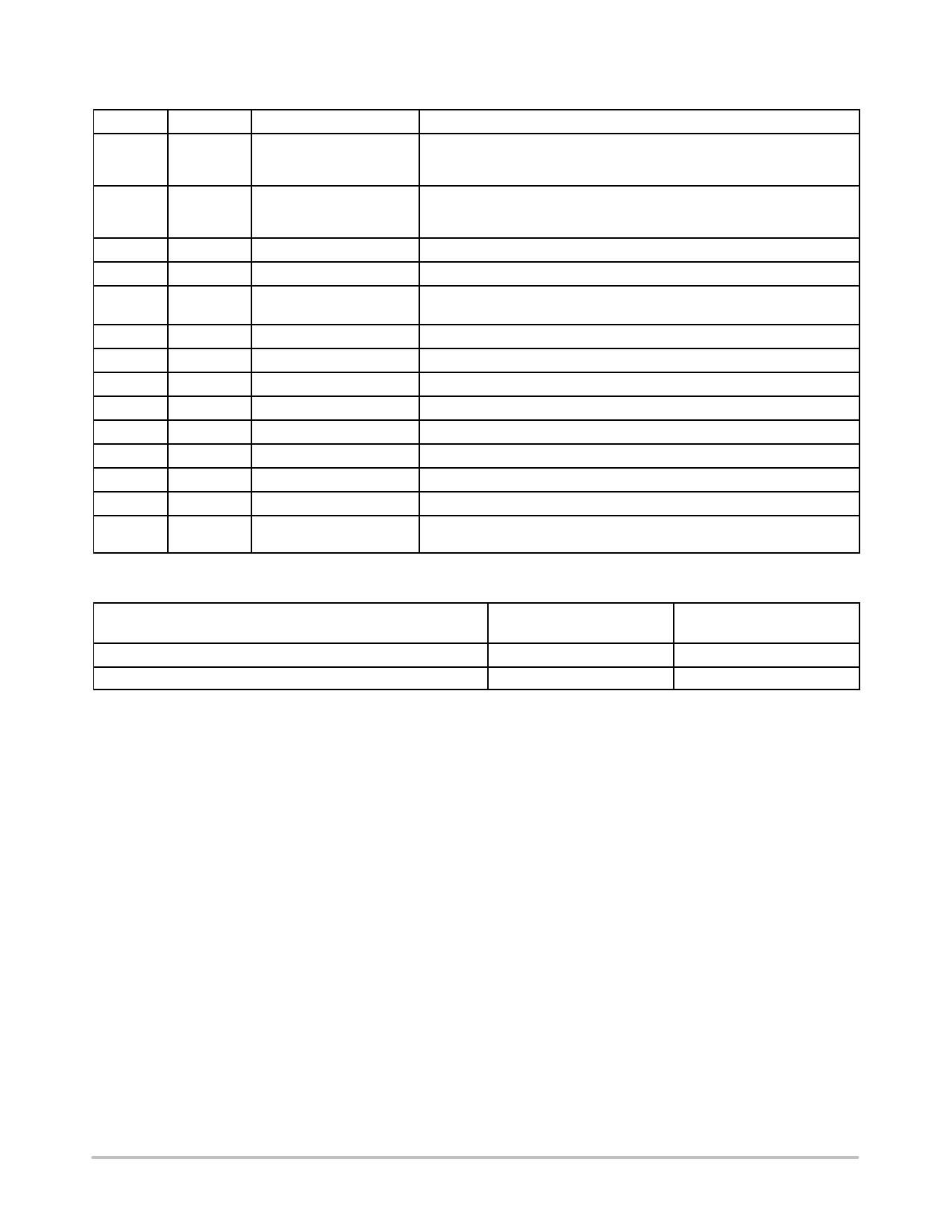
PIN FUNCTION DESCRIPTION
Pin No. Pin Name
Function
1
OPP
Adjust the Over Power
Protection
2
OTP
Over−Temperature
Protection
3
Timer
Timer
4
ZCD
Zero Crossing Detection
5
Ct
Timing Capacitor
6
FB
Feedback Pin
7
CS
Current Sense
8
GND
−
9
DRV
Driver Output
10
VCC
Supplies the Controller
11
BO
Brownout
12
OVP
Over−Voltage Protection
13
NC
−
14
HV
High−Voltage Input
Pin Description
A negative voltage applied to this pin reduces the internal maximum peak
current setpoint. Connecting it to an auxiliary winding through a resistor
divider thus performs Over Power compensation. If grounded, OPP is null.
Connect an NTC between this pin and GND pin. Pin 2 features an internal
current source that biases the NTC. When the NTC pulls the pin down, the
circuit permanently latches−off.
Wiring a capacitor to ground helps selecting the timer duration.
Connected to the auxiliary winding, this pin detects the core reset event.
A capacitor connected to this pin acts as the timing capacitor in foldback
mode.
Hooking an optocoupler collector to this pin will allow regulation.
This pin monitors the primary peak current.
This pin is the controller ground.
This pin is the driver’s output to an external MOSFET.
This pin is connected to an external auxiliary voltage.
This pin is the brownout input.
By pulling this pin high, the controller can be permanently latched−off.
This pin is omitted for improved creepage.
Connected to the bulk capacitor, this pin powers the internal current source
to deliver a startup current.
OVERCURRENT PROTECTION ON NCP1336 VERSIONS
NCP1336 / A
NCP1336 / B
Auto−Recovery
Overcurrent protection
X
Latched
Overcurrent protection
X
http://onsemi.com
2
Share Link: