MT8941B 데이터 시트보기 (PDF) - Mitel Networks
부품명
상세내역
일치하는 목록
MT8941B Datasheet PDF : 22 Pages
| |||
MT8941B CMOS
Functional Description
The MT8941B is a dual digital phase-locked loop
providing the timing and synchronization signals to
the interface circuits for T1 and CEPT (30+2)
Primary Multiplex Digital Transmission links. As
shown in the functional block diagram (see Figure 1),
the MT8941B has two digital phase-locked loops
(DPLLs), associated output controls and the mode
selection logic circuits. The two DPLLs, although
similar in principle, operate independently to provide
T1 (1.544 MHz) and CEPT (2.048 MHz) transmission
clocks and ST-BUS timing signals.
The principle of operation behind the two DPLLs is
shown in Figure 3. A master clock is divided down to
8 kHz where it is compared with the 8 kHz input, and
depending on the output of the phase comparison,
the master clock frequency is corrected.
Master clock
(12.352 MHz /
16.384 MHz)
Frequency
Correction
Input (8 kHz)
Phase
Comparison
÷8
Output
(1.544 MHz /
2.048 MHz)
÷ 193 /
÷ 256
Figure 3 - DPLL Principle
The MT8941B achieves the frequency correction in
both directions by using three methods; speed-up,
slow-down and no-correction.
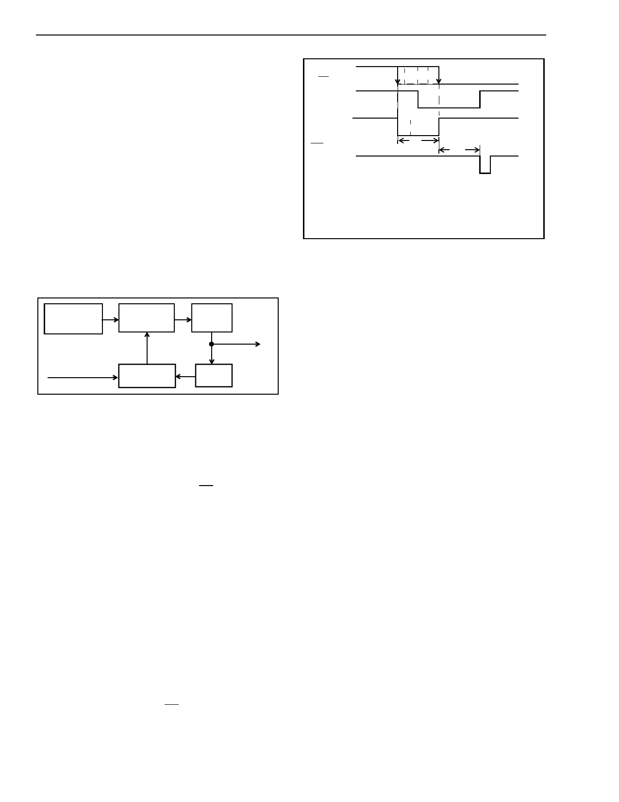
As shown in Figure 4, the falling edge of the 8 kHz
input signal (C8Kb for DPLL #2 or F0i for DPLL # 1)
is used to sample the internally generated 8 kHz
clock and the correction signal (CS) once in every
frame (125 µs). If the sampled CS is “1”, then the
DPLL makes a speed-up or slow-down correction
depending upon the sampled value of the internal 8
kHz signal. A sampled ”0” or “1” causes the
frequency correction circuit to respectively stretch or
shrink the master clock by half a period at one
instant in the frame. If the sampled CS is “0”, then
the DPLL makes no correction on the master clock
input. Note that since the internal 8 kHz signal and
the CS signal are derived from the master clock, a
correction will cause both clocks to stretch or shrink
simultaneously by an amount equal to half the period
of the master clock.
Once in synchronization, the falling edge of the
reference signal (C8Kb or F0i) will be aligned with
either the falling or the rising edge of CS. It is aligned
with the rising edge of CS when the reference signal
is slower than the internal 8 kHz signal. On the other
hand, the falling edge of the
4
C8Kb (DPLL #2)
or F0i (DPLL #1)
Internal
8 kHz
correction
CS
speed-up
region
F0b
(DPLL #2)
tCS
no-correction
sampling edge
correction
slow-down
region
tCSF
DPLL #1: tCS = 4 × TP12 ± 0.5 × TP12
DPLL #2: tCS = 512 × TP16 ± 0.5 × TP16
tCSF = 766 × TP16
where, TP12 is the 12.352 MHz master clock oscillator period
for DPLL #1 and TP16 is the 16.384 MHz master clock period
for DPLL #2.
Figure 4 - Phase Comparison
reference signal will be aligned with the falling edge
of CS if the reference signal is faster than the
internal 8 kHz signal.
Input-to-Output Phase Relationship
The no-correction window size is 324 ns for DPLL #1
and 32 µs for DPLL #2. It is possible for the relative
phase of the reference signal to swing inside the no-
correction window depending on its jitter and the
relative drift of the master clock. As a result, the
phase relationship between the input signal and the
output clocks (and frame pulse in case of DPLL #2)
may vary up to a maximum of window size. This
situation is illustrated in Figure 4. The maximum
phase variation for DPLL #1 is 324 ns and for DPLL
#2 it is 32µs. However, this phase difference can be
absorbed by the input jitter buffer of Mitel’s T1/CEPT
devices.
The no-correction window acts as a filter for low
frequency jitter and wander since the DPLL does not
track the reference signal inside it. The size of the
no-correction window is less than or equal to the size
of the input jitter buffer on the T1 and CEPT devices
to guarantee that no slip will occur in the received
T1/CEPT frame.
The circuit will remain in synchronization as long as
the input frequency is within the lock-in range of the
DPLLs (refer to the section on “Jitter Performance
and Lock-in Range” for further details). The lock-in
range is wide enough to meet the CCITT line rate
specification (1.544 MHz ±32 ppm and 2.048 MHz
±50 ppm) for the High Capacity Terrestrial Digital
Service.
The phase sampling is done once in a frame (8 kHz)
for each DPLL. The divisions are set at 8 and 193 for
DPLL #1, which locks to the falling edge of the input
Share Link: 