MC145540 데이터 시트보기 (PDF) - Motorola => Freescale
부품명
상세내역
일치하는 목록
MC145540 Datasheet PDF : 116 Pages
| |||
2.2.7.2 SHORT FRAME SYNC
Short Frame Sync is the industry name for this type of clocking format which controls the transfer of the
ADPCM data words. Refer to Section 2.4.3, Figure 2-7. This device uses Short Frame Sync timing for
32 kbps ADPCM only. The “Frame Sync” or “Enable” is used for two specific synchronizing functions.
The first is to synchronize the ADPCM data word transfer, and the second is to control the internal
analog-to-digital and digital-to-analog conversions. The term “Sync” refers to the function of synchro-
nizing the ADPCM data word onto or off of the multiplexed serial ADPCM data bus, also known as a
PCM highway. The term “Short” comes from the duration of the frame sync measured in PCM data clock
cycles. Short Frame Sync timing occurs when the frame sync is used as a “pre-synchronization” pulse
that is used to tell the internal logic to clock out the ADPCM data word under complete control of the data
clock. The Short Frame Sync is held high for one falling data clock edge. The device outputs the
ADPCM data word beginning with the following rising edge of the data clock. This results in the ADPCM
output going low impedance with the rising edge of the transmit data clock, and remaining low imped-
ance until the middle of the LSB (three and a half PCM data clock cycles).
The device recognizes Short Frame Sync clocking when the frame sync is held high for one and only
one falling edge of the transmit data clock. The transmit logic decides on each frame sync whether it
should interpret the next frame sync pulse as a Long or a Short Frame Sync. It is not recommended to
switch between Long Frame Sync and Short Frame Sync clocking without going through a power down
cycle due to bus contention problems. The device is designed to prevent PCM bus contention by not
allowing the ADPCM data output to go low impedance for at least two frame sync cycles after power is
applied or when coming out of a power-down mode.
The receive side of the device is designed to accept the same frame sync and data clock as the transmit
side and to be able to latch its own transmit ADPCM data word. Thus the PCM digital switch only needs
to be able to generate one type of frame sync for use by both transmit or receive sections of the device.
The falling edge of the receive data clock (BCLKR) latching a high logic level at the receive frame sync
(FSR) input tells the device to start latching the 4-bit ADPCM serial word into the receive data input on
the following four falling edges of the receive data clock. The internal receive logic counts the receive
data clock cycles and transfers the ADPCM data word to a register for access by the DSP.
When the device is programmed to be in the PCM Codec mode by BR0 (4:3), the device will output the
complete 8-bit PCM word using the short frame sync clocking format. The 8-bit PCM word will be
clocked out (or in) the same way that the 4-bit ADPCM word would be, except that the fourth bit will be
valid for the full BCLKT period and the eighth bit will be valid for only one half of the BCLKT period.
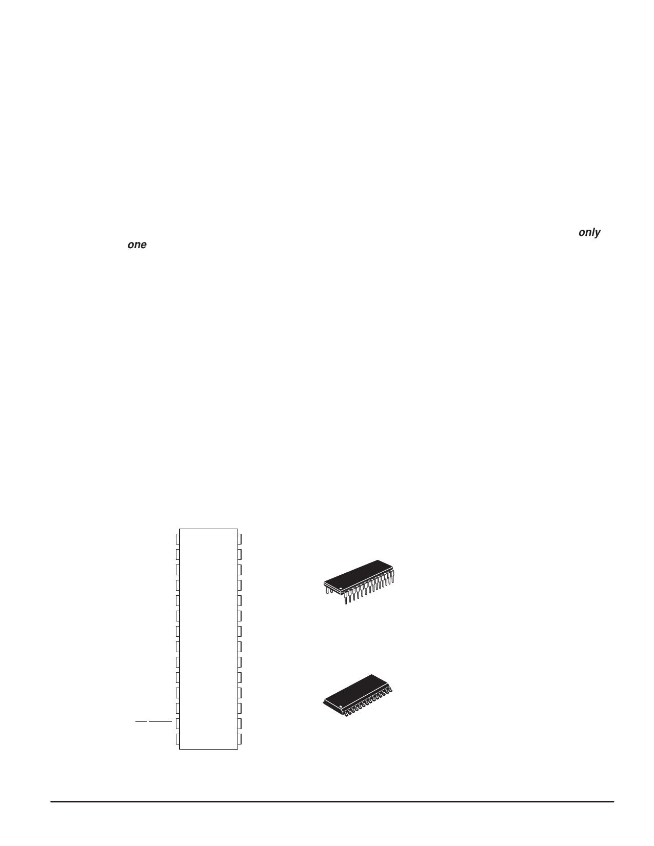
2.3 PIN ASSIGNMENT
The pin assignments for the MC145540 28-lead DIP and SOG packages are shown in Figure 2-2.
• TG
1
TI -
2
TI+
3
VAG
4
RO
5
AXO -
6
AXO +
7
VDSP
8
VEXT
9
PI 10
PO - 11
PO + 12
PDI/RESET 13
SCP EN 14
28
VDD
27
FSR
26
BCLKR
25
DR
24
C1+
23
C1-
22
VSS
21
SPC
20
DT
19
BCLKT
18
FST
17
SCP Rx
16
SCP Tx
15
SCP CLK
(TOP VIEW)
28
1
28
1
MC145540P
28-LEAD PLASTIC DIP
CASE 710
MC145540DW
28-LEAD WIDE BODY SOG
CASE 751F
Figure 2-2. Pin Assignments
2-10
MC145540
MOTOROLA
Share Link: 