ADG508F 데이터 시트보기 (PDF) - Analog Devices
부품명
상세내역
일치하는 목록
ADG508F Datasheet PDF : 12 Pages
| |||
ADG508F/ADG509F/ADG528F
TERMINOLOGY
VDD
VSS
GND
RON
RON Drift
RON Match
IS (OFF)
ID (OFF)
ID, IS (ON)
VD (VS)
CS (OFF)
CD (OFF)
CD, CS (ON)
CIN
tON (EN)
tOFF (EN)
tTRANSITION
tOPEN
VINL
VINH
IINL (IINH)
Off Isolation
Charge Injection
IDD
ISS
Most positive power supply potential.
Most negative power supply potential.
Ground (0 V) reference.
Ohmic resistance between D and S.
Change in RON when temperature changes
by one degree Celsius.
Difference between the RON of any two
channels.
Source leakage current when the switch is
off.
Drain leakage current when the switch is off.
Channel leakage current when the switch is
on.
Analog voltage on terminals D, S.
Channel input capacitance for “OFF”
condition.
Channel output capacitance for “OFF”
condition.
“ON” switch capacitance.
Digital input capacitance.
Delay time between the 50% and 90% points
of the digital input and switch “ON”
condition.
Delay time between the 50% and 90% points
of the digital input and switch “OFF”
condition.
Delay time between the 50% and 90% points
of the digital inputs and the switch “ON”
condition when switching from one address
state to another.
“OFF” time measured between 80% points of
both switches when switching from one
address state to another.
Maximum input voltage for Logic “0”.
Minimum input voltage for Logic “1”.
Input current of the digital input.
A measure of unwanted signal coupling
through an “OFF” channel.
A measure of the glitch impulse transferred
from the digital input to the analog output
during switching.
Positive supply current.
Negative supply current.
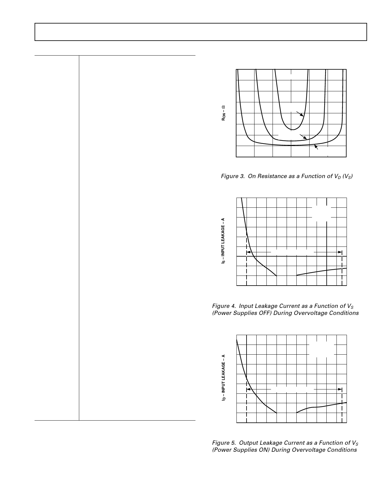
Typical Performance Graphs
2000
1750
TA = +25؇C
1500
1250
1000
VDD = +5V
VSS = –5V
750
500
250
0
–15
–10
VDD = +10V
VSS = –10V
–5
0
5
VD (VS) – Volts
VDD = +15V
VSS = –15V
10
15
Figure 3. On Resistance as a Function of VD (VS)
1m
100
10
1
VDD = 0V
VSS = 0V
VD = 0V
100n
10n
OPERATING RANGE
1n
100p
10p
1p
–50 –40 –30 –20 –10 0 10 20 30 40 50 60
VIN – INPUT VOLTAGE – Volts
Figure 4. Input Leakage Current as a Function of VS
(Power Supplies OFF) During Overvoltage Conditions
1m
100
10
1
VDD = +15V
VSS = –15V
VD = 0V
100n
10n
OPERATING RANGE
1n
100p
10p
1p
–50 –40 –30 –20 –10 0 10 20 30 40 50 60
VIN – INPUT VOLTAGE – Volts
Figure 5. Output Leakage Current as a Function of VS
(Power Supplies ON) During Overvoltage Conditions
REV. C
–5–
Share Link: 