ADG508F 데이터 시트보기 (PDF) - Analog Devices
부품명
상세내역
일치하는 목록
ADG508F Datasheet PDF : 12 Pages
| |||
ADG508F/ADG509F/ADG528F
Table I. ADG508F Truth Table
Table II. ADG509F Truth Table
A2
A1
A0
EN
ON SWITCH
A1
A0
EN
ON SWITCH PAIR
X
X
X
0
NONE
0
0
0
1
1
0
0
1
1
2
0
1
0
1
3
0
1
1
1
4
1
0
0
1
5
1
0
1
1
6
1
1
0
1
7
1
1
1
1
8
X
X
0
0
0
1
0
1
1
1
0
1
1
1
1
X = Don’t Care
NONE
1
2
3
4
X = Don’t Care
Table III. ADG528F Truth Table
ON
A2
A1
A0
EN WR RS SWITCH
X
X
X
X
g
1
Retains Previous Switch Condition
X
X
X
X
X
0
NONE (Address and Enable Latches Cleared)
X
X
X
0
0
1
NONE
0
0
0
1
0
1
1
0
0
1
1
0
1
2
0
1
0
1
0
1
3
0
1
1
1
0
1
4
1
0
0
1
0
1
5
1
0
1
1
0
1
6
1
1
0
1
0
1
7
1
1
1
1
0
1
8
X = Don’t Care
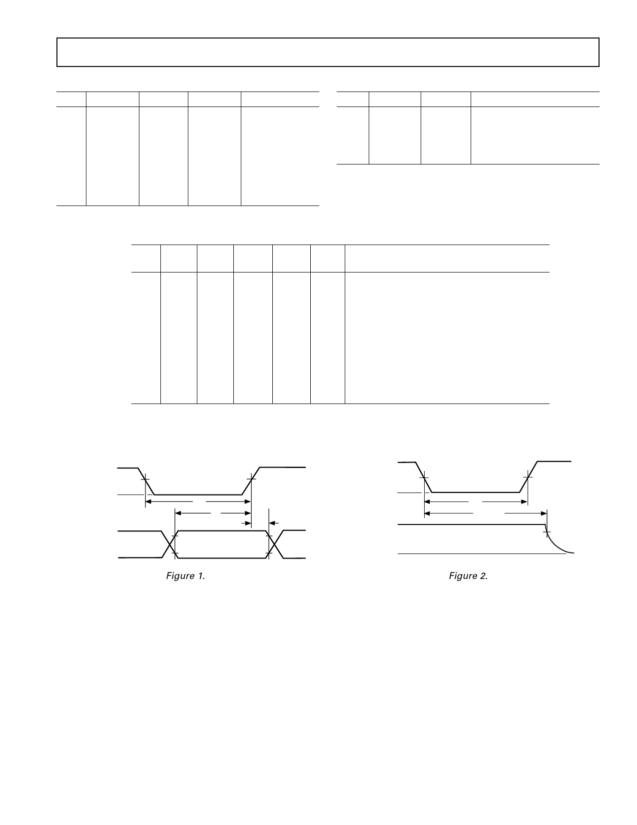
TIMING DIAGRAMS (ADG528F)
3V
WR
0V
3V
A0, A1, A2
EN
0V
50%
50%
tW
tS
2V
tH
0.8V
Figure 1.
Figure 1 shows the timing sequence for latching the switch
address and enable inputs. The latches are level sensitive; there-
fore, while WR is held low, the latches are transparent and the
switches respond to the address and enable inputs. This input
data is latched on the rising edge of WR.
3V
RS
0V
VO
SWITCH
OUTPUT
0V
50%
50%
tRS
tOFF (RS)
0.8VO
Figure 2.
Figure 2 shows the Reset Pulsewidth, tRS, and the Reset Turn-
off Time, tOFF (RS).
Note: All digital input signals rise and fall times are measured
from 10% to 90% of 3 V. tR = tF = 20 ns.
REV. C
–3–
Share Link: 