AD5764(RevPrC) 데이터 시트보기 (PDF) - Analog Devices
부품명
상세내역
일치하는 목록
AD5764
(Rev.:RevPrC)
(Rev.:RevPrC)
Analog Devices

AD5764 Datasheet PDF : 27 Pages
| |||
Preliminary Technical Data
AD5764
68HC11*
MOSI
SCK
PC7
PC6
MISO
AD5764*
SDIN
SCLK
SYNC
LDAC
SDO
SDIN
AD5764*
SCLK
SYNC
LDAC
SDO
R
SDIN
AD5764*
SCLK
SYNC
LDAC
SDO
*ADDITIONAL PINS OMITTED FOR CLARITY
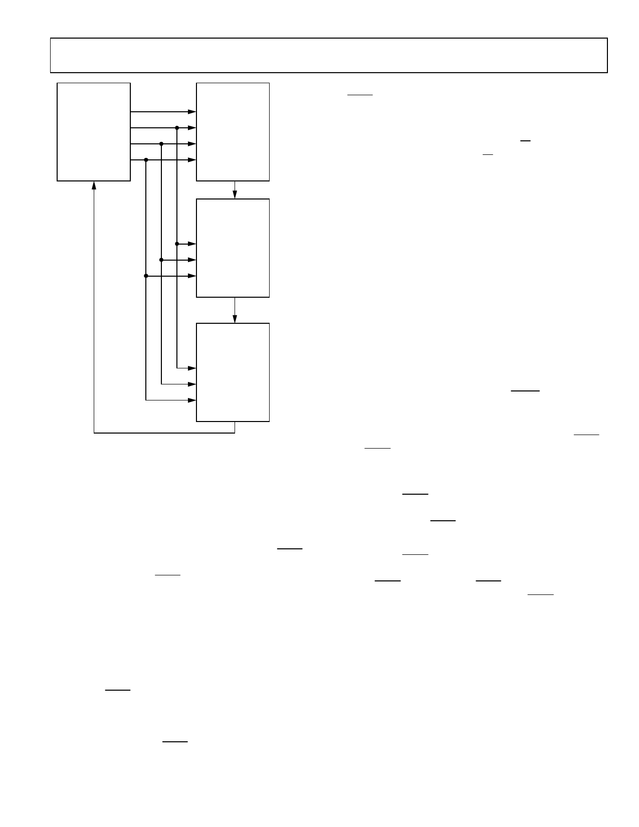
Figure 8. Daisy chaining the AD5764
Daisy-Chain Operation
For systems that contain several devices, the SDO pin may be
used to daisy-chain several devices together. This daisy-chain
mode can be useful in system diagnostics and in reducing the
number of serial interface lines. The first falling edge of SYNC
starts the write cycle. The SCLK is continuously applied to the
input shift register when SYNC is low. If more than 24 clock
pulses are applied, the data ripples out of the shift register and
appears on the SDO line. This data is clocked out on the rising
edge of SCLK and is valid on the falling edge. By connecting the
SDO of the first device to the DIN input of the next device in
the chain, a multidevice interface is constructed. Each device in
the system requires 24 clock pulses. Therefore, the total number
of clock cycles must equal 24N, where N is the total number of
AD5764s in the chain. When the serial transfer to all devices is
complete, SYNC is taken high. This latches the input data in
each device in the daisy chain and prevents any further data
from being clocked into the input shift register. The serial clock
may be a continuous or a gated clock. A continuous SCLK
source can only be used if SYNC is held low for the correct
number of clock cycles. In gated clock mode, a burst clock
containing the exact number of clock cycles must be used and
SYNC must be taken high after the final clock to latch the data.
Readback Operation
Readback mode is invoked by setting the R/W bit = 1 in the
serial input register write. With R/W = 1, Bits A2–A0, in
association with Bits REG2 , REG1, and REG0, select the
register to be read. The remaining data bits in the write
sequence are don’t cares. During the next SPI write, the data
appearing on the SDO output will contain the data from the
previously addressed register. For a read of a single register, the
NOP command can be used in clocking out the data from the
selected register on SDO. The readback diagram in Figure 4
shows the readback sequence. For example, to read back the
fine gain register of Channel A on the AD5764, the following
sequence should be implemented. First, write 0xA0XXXX to
the AD5764 input register. This configures the AD5764 for read
mode with the fine gain register of Channel A selected. Note
that all the data bits, D15 to D0, are don’t cares. Follow this with
a second write, a NOP condition, 0x00XXXX. During this
write, the data from the fine gain register is clocked out on the
SDO line, i.e., data clocked out will contain the data from the
fine gain register in Bits D5 to D0.
SIMULTANEOUS UPDATING VIA LDAC
After data has been transferred into the input register of the
DACs, there are two ways in which the DAC registers and DAC
outputs can be updated. Depending on the status of both SYNC
and LDAC, one of two update modes is selected.
Individual DAC Updating
In this mode, LDAC is held low while data is being clocked into
the input shift register. The addressed DAC output is updated
on the rising edge of SYNC.
Simultaneous Updating of All DACs
In this mode, LDAC is held high while data is being clocked
into the input shift register. All DAC outputs are updated by
taking LDAC low any time after SYNC has been taken high.
The update now occurs on the falling edge of LDAC.
Rev. PrC 21-Oct-04| Page 17 of 28
Share Link: