NJU3962E2 데이터 시트보기 (PDF) - Japan Radio Corporation
부품명
상세내역
일치하는 목록
NJU3962E2 Datasheet PDF : 11 Pages
| |||
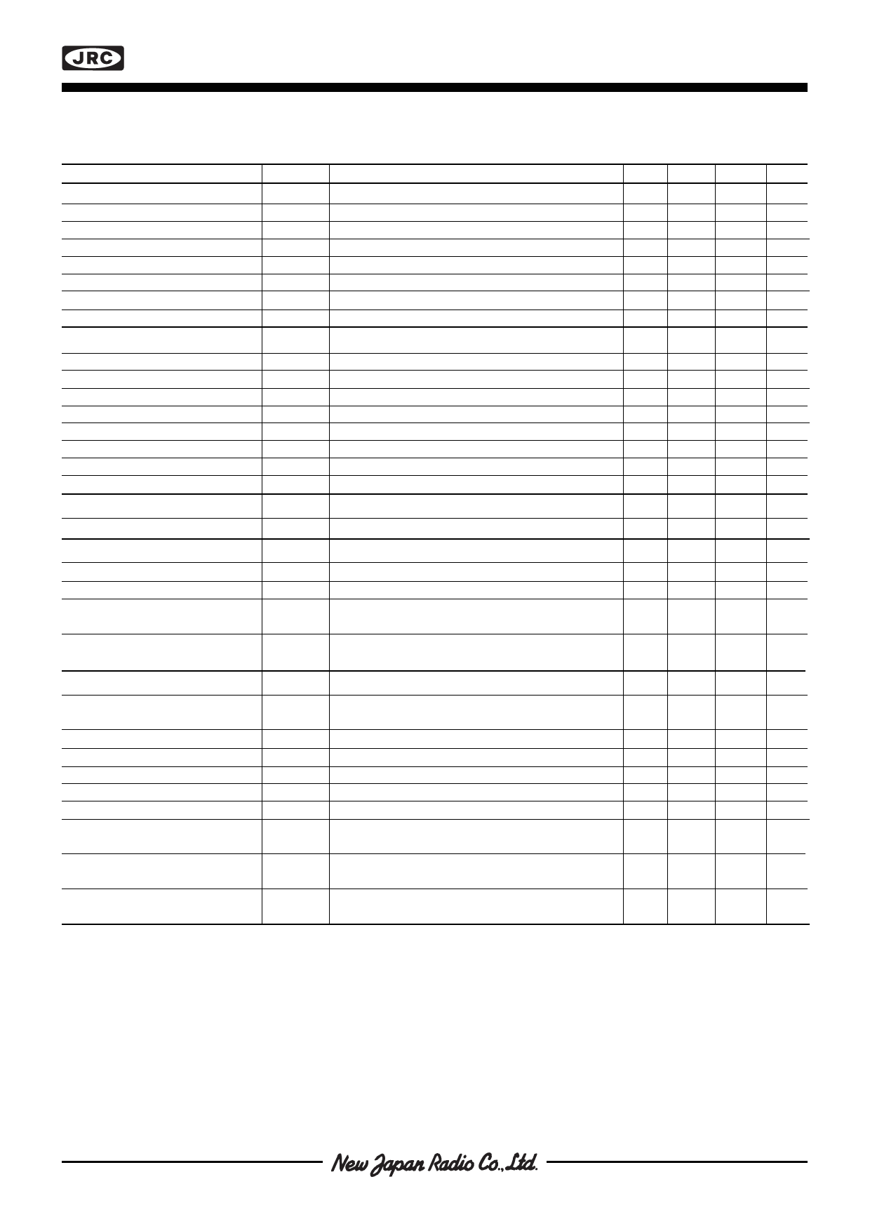
s ELECTRICAL CHARACTERISTICS
Electrical characteristics over recommended operating conditions.
Parameter
Logic Input
Reset logic HIGH input voltage
Reset logic LOW input voltage
Logic HIGH input voltage
Logic LOW input voltage
Reset input current
Input current, other inputs
Input capacitance
Internal Timing Characteristics
Address setup time
Data setup time
Chip select setup time
Address hold time
Data hold time
Chip select hold time
Write cycle length
Reset cycle length
Reference Input
Input resistance
Logic Outputs
Logic HIGH output current
Logic LOW output current
Write propagation delay
Symbol
VIHR
VILR
V
IH
V
IL
IIR
I
I
t
as
t
ds
tcs
tah
tdh
tch
tWR
t
res
Rref
IOH
I
OL
t
pwr
Reset propagation delay
tpres
DAC Outputs
Nominal output voltage
V
DA
Conditions
VSS < VIR < VDD
V <V<V
SS
I
DD
Valid for A0
Valid for D0 - D7
VO = 2.4 V
V = 0.4 V
O
From positive edge of WR.
Outputs valid, Cload = 120 pF
From positive edge of Reset to
outputs valid, Cload = 120 pF
Reset open, VRef = 2.5 V
Resolution
Offset error
Gain error
Endpoint nonlinearity
Differential nonlinearity
Load error
Power supply sensitivity
Conversion speed
(V , unloaded - V , loaded)
DA
DA
Rload = 2.5 kohm, Code 127 to DAC
Code 127 to DAC
4.75 V < VDD < 5.25 V
tDAC For a full-scale transition to ±0.5 LSB
of final value, Rload = 2.5 kohm, Cload = 50 pF.
NJU39612
Min
Typ
3.5
-
-
-
2.0
-
-
-
-0.01 -
-1
-
-
3
Max Unit
-
V
0.1 V
-
V
0.8 V
1 mA
1
µA
-
pF
60
-
60
-
70
-
-
-
-
-
-
-
50
-
80
-
-
ns
-
ns
-
ns
0
ns
0
ns
0
ns
-
ns
-
ns
6
9
- kohm
-
-13
-5 mA
2
5
- mA
-
30 100 ns
-
60 150 ns
0
-
V
Ref
- 1LSB V
-
7
- Bits
-
0.2
0.5 LSB
-
0.1
0.5 LSB
-
0.2
0.5 LSB
-
0.2
0.5 LSB
-
0.1
0.5 LSB
-
0.1
0.3 LSB
-
3
8
µs
Share Link: 