NJU3962E2 데이터 시트보기 (PDF) - Japan Radio Corporation
부품명
상세내역
일치하는 목록
NJU3962E2 Datasheet PDF : 11 Pages
| |||
NJU39612
Current Direction, Sign1 & Sign2
These bits are transferred from D when writing in the respective DA register. A must be set according to the data
7
0
transfer table in figure 7.
DA1 and DA2
These are the two outputs of DAC1 and DAC2. Input to the DACs are internal data bus (Q61 … Q01) and (Q62 … Q02).
Reference Voltage V
Ref
VRef is the analog input for the two DACs. Special care in layout, gives a very low voltage drop from pin to resistor.
Any VRef between 0.0 V and VDD can be applied, but output might be non-linear above 3.0 V.
Power-on Reset
This function automatically resets all internal flip flops at power-on. This results in VSS voltage at both DAC outputs
and all digital outputs.
Reset
If Reset is not used, leave it disconnected. Reset can be used to measure leakage currents from VDD.
I2 [mA]
I
T max
T2 [mNm]
Tnom
Tmin
I1 [mA]
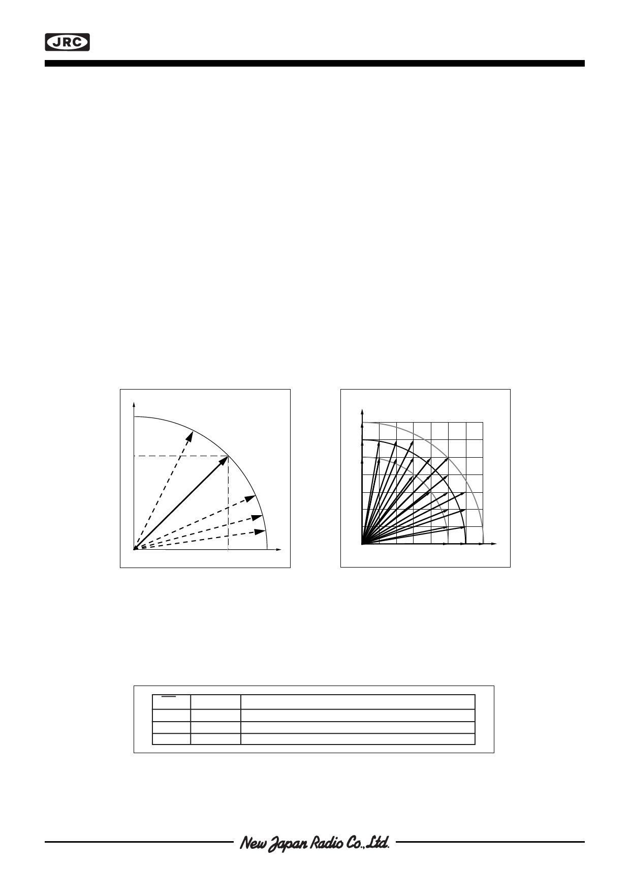
Figure 6a. Assuming that torque is
proportional to the current in resp.
winding it is possible to draw figure
8b.
T1
[mNm]
Figure 6b. An example of acces-
sible positions with a given torque
deviation/fullstep. Note that 1:st
µstep sets highest resolution. Data
points are exaggerated for illustra-
tion purpose.
TNom = code 127.
CS
A0
0
0
0
1
1
X
Data Transfer
D7 —> Sign1, (D6—D0) —> (Q61—Q01)
D7 —> Sign2, (D6—D0) —> (Q62—Q02)
No Transfer
Figure 7. Table showing how data is transfered inside NJU39612.
Share Link: 