SCY99080CDWR2G 데이터 시트보기 (PDF) - ON Semiconductor
부품명
상세내역
일치하는 목록
SCY99080CDWR2G
ON Semiconductor

SCY99080CDWR2G Datasheet PDF : 27 Pages
| |||
DDA002C
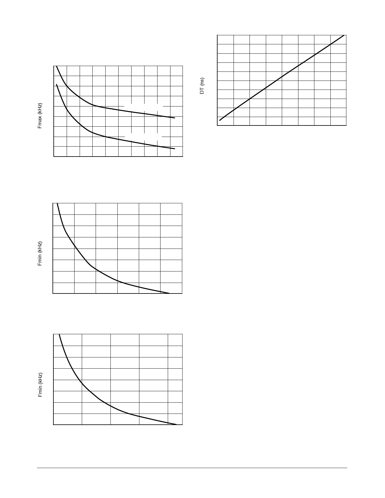
The selection of the three setting resistors (Fmax, Fmin and
deadtime) require the usage of the selection charts displayed
below:
500
450
400
350
300
Fmin = 200 kHz
250
200
150
Fmin = 30 kHz
100
50
2 4 6 8 10 12 14 16 18 20 22
RFmax (kW)
Figure 38. Maximum Switching Frequency
Resistor Selection Depending on the Adopted
Minimum Switching Frequency
100
90
80
70
60
50
40
30
20
20
40
60
80
100
RFmin (kW)
120 140
Figure 39. Minimum Switching Frequency Resistor
Selection (Fmin = 20 kHz to 100 kHz)
500
450
400
350
300
250
200
150
100
2
7
12
17
22
RFmin (kW)
Figure 40. Minimum Switching Frequency Resistor
Selection (Fmin = 100 kHz to 500 kHz)
2000
1800
1600
1400
1200
1000
800
600
400
200
0
1 11 21 31 41 51 61 71 81
Rdt (kW)
Figure 41. Deadtime Resistor Selection
Deadtime Control
Deadtime control is an absolute necessity when the
half−bridge configuration comes into play. The deadtime
technique consists of including a time period during which
both high and low side switches are off. Of course, the
deadtime amount should be different depending on the
switching frequency, hence the ability to adjust it on this
controller. The option ranges between 100 ns and 2 ms. The
deadtime is actually made by the internal timer which is a
part of the VCO. Please refer to Figures 35 and 37 for more
details. During the Ct_DT capacitor charge time, the internal
latch is set and invalidates the AND gates: all outputs are
low. When the comparator goes back to the low level, A and
B outputs are validated, while the timing capacitor Ct_T_On
recharges. By connecting a resistor RDT to the ground, it
creates a current whose image serves to charge the Ct_DT
capacitor − we control the deadtime. It typically ranges
between 100 ns (RDT = 2.7 kW) and 2 ms (RDT = 70 kW).
100 ms PFC Timer
The DDA002C device features an internal digital timer
that prolongs the device start by 100 ms after the controller
is enabled by Vccon and/or a BO event. This fixed delay
allows the PFC stage to fully stabilize the bulk voltage
before the resonant power stage is activated. The PFC delay
also occurs when the EN2 input is released.
Adjustable Preheat Period − CIG Timer
As this IC is tailored not only for the resonant SMPS
applications but also to drive HCFL lamp ballasts, it
includes an adjustable preheat timer that allows the designer
to accurately setup needed filament preheat time. The timer
uses an external capacitor (Cpreheat) that is charged from an
internal current source (CIG_I). The IC outputs are forced
(via VCO) to operate at the frequency that is given by the
parallel combination of resistors Rfmin and Rfstart until the
Cpreheat capacitor voltage reaches 5 V. Figure 42 shows the
internal arrangement of the GIC timer.
http://onsemi.com
18
Share Link: