SCY99080CDWR2G 데이터 시트보기 (PDF) - ON Semiconductor
부품명
상세내역
일치하는 목록
SCY99080CDWR2G
ON Semiconductor

SCY99080CDWR2G Datasheet PDF : 27 Pages
| |||
DDA002C
400 11V
10V
Vbulk = 350 V
300 8V
Vbulk = 250 V
6V
200
4V
100
2V
>>
0V 0V
0s 5us 10us 15us 20us 25us 30us 35us 40us
Time
Figure 46. Simulation Results for 350/250
ON/OFF Brown Out Levels
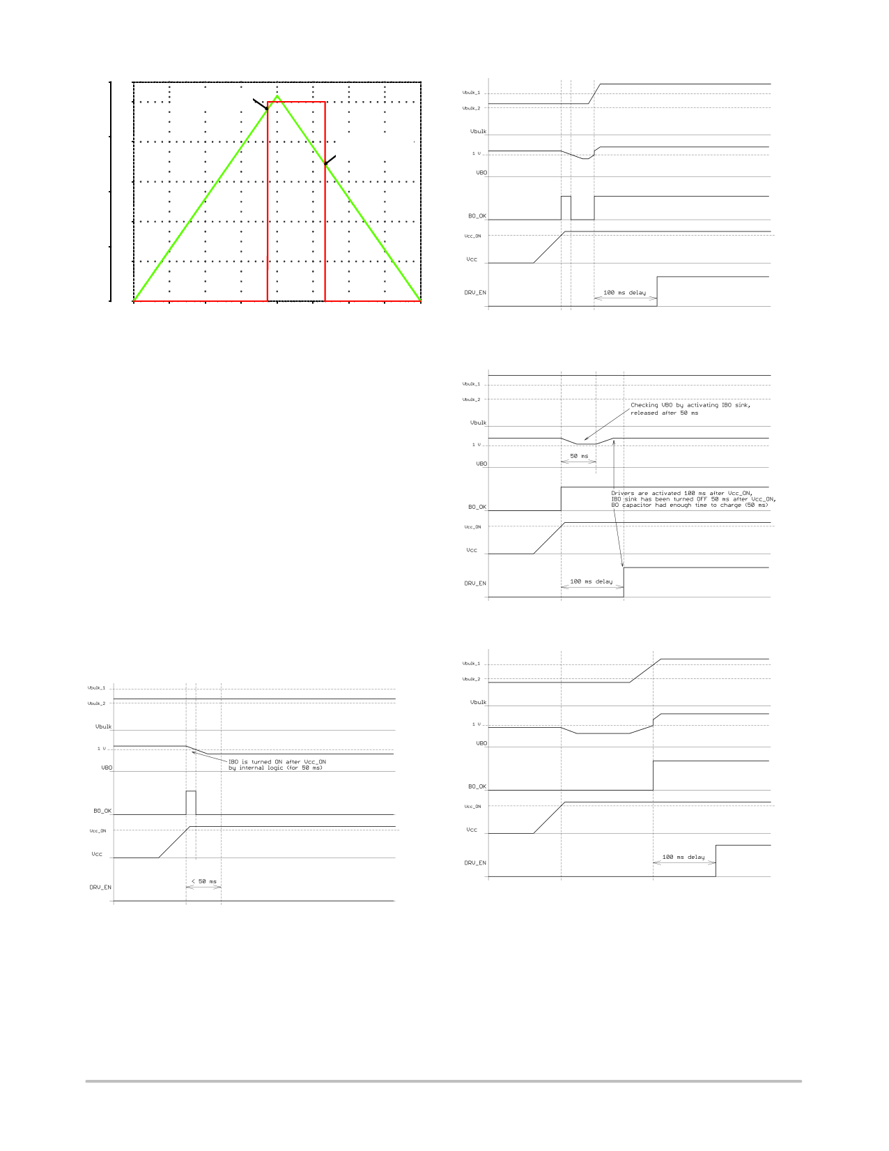
Note that the brown−out input will disable the controller
operation anytime its voltage goes below 1 V threshold. A
20 ms filter is used to improve the noise immunity of this
input. The full start−up sequence (i.e. PFC delay, preheat and
soft start) is provided by the controller in case the BO input
is re−enabled.
The IBO current sink is turned ON for 50 ms after any
controller restart to let the BO input voltage stabilize (big
capacitor can be connected to the BO input and the IBO is
only 20 mA so it will take some time to discharge). Once the
50 ms one shoot pulse ends the BO comparator is supposed
to either hold the IBO sink turned ON (if the bulk voltage
level is not sufficient) or turn it OFF (if the bulk voltage is
higher than Vbulk1).
See Figures 47 − 50 for better understanding on how the
BO input works.
Figure 48. BO Input Functionality −
Vbulk2 < Vbulk < Vbulk1, PFC Start Follows
Figure 49. BO Input Functionality − Vbulk > Vbulk1
Figure 47. BO Input Functionality −
Vbulk2 < Vbulk < Vbulk1
Figure 50. BO Input Functionality −
Vbulk < Vbulk2, PFC Start Follows
http://onsemi.com
21
Share Link: