SCY99080CDWR2G 데이터 시트보기 (PDF) - ON Semiconductor
부품명
상세내역
일치하는 목록
SCY99080CDWR2G
ON Semiconductor

SCY99080CDWR2G Datasheet PDF : 27 Pages
| |||
DDA002C
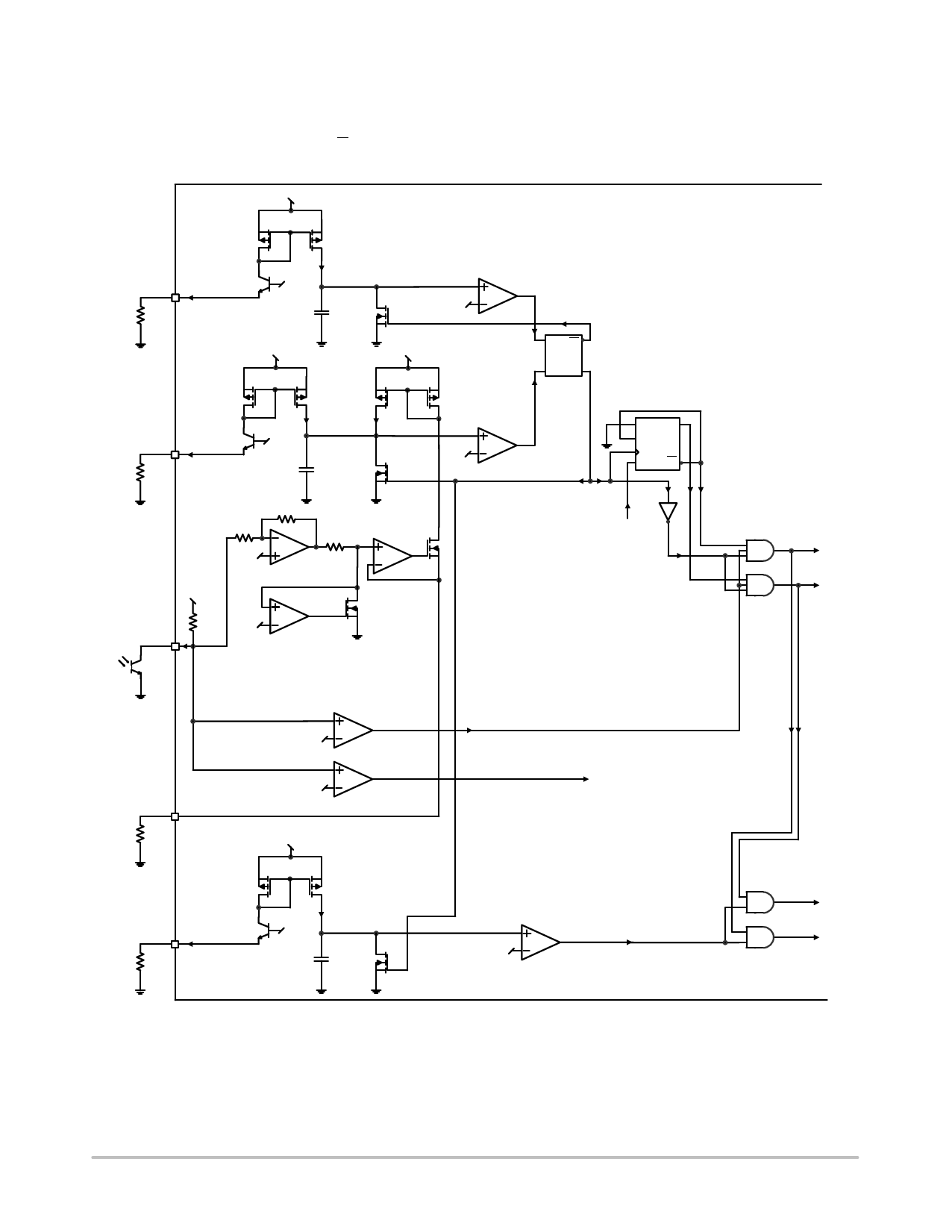
Voltage−Controlled Oscillator
The VCO section features a high−speed circuitry allowing
operation from 60 kHz up to 1 MHz. However, as there is an
internal division by two, it creates Q and Q outputs. The final
effective signal on the outputs Lgd, Hgd, Lgs and Hgs
Vdd
therefore switches between 30 kHz and 500 kHz. The VCO
is configured in such a way that if the feedback pin voltage
goes down, the switching frequency goes up. Figure 35
shows simplified architecture of the VCO.
DT
Vref
Vref = 2.5 V
Ct_DT
Vdd
Vdd
RQ
SQ
Rfmin
Vref
Ct_ T_On
Vref = 2.5 V
Vref = 1.2 V
Vdd
10 k
FB
Vref = 1.2 V
SQ
D
CLK
RQ
DT
from
internal logic
B
To drivers
A
Vref_DC_0 = 1.2 V
R_Fmax
Vref_FB_Fault = 6 V
Vdd
Skip
FB_Fault
To_FB_Fault_Timer
Dgs
Vref
On_time_clamp
Vref = 2.5 V
Ct_Dgs
SR_B
To SR drivers
SR_A
Figure 35. Simplified VCO Architecture
The VCO conversion characteristic is shown in Figure 36.
The FB fault is detected in case the feedback voltage is
higher than 6 V. This will happen if the converter is
overloaded or the feedback path is not closed i.e. a broken
optocoupler. The internal fault timer starts to count once the
FB fault is detected and it latches off the controller if the fault
lasts more than 50 ms. To overcome triggering of the FB
fault protection during the application start, the FB timer is
disabled until the soft−start period ends (VSS > 1.9 V).
http://onsemi.com
16
Share Link: