NCV8184(2019) 데이터 시트보기 (PDF) - ON Semiconductor
부품명
상세내역
일치하는 목록
NCV8184 Datasheet PDF : 20 Pages
| |||
NCV8184
CIRCUIT DESCRIPTION
ENABLE Function
By pulling the VREF/ENABLE lead below 0.8 V, (see
Figure 16 or Figure 17), the IC is disabled and enters a sleep
state where the device draws less than 20 mA from supply.
When the VREF/ENABLE lead is greater than 2.1 V, VOUT
tracks the VREF/ENABLE lead normally.
Output Voltage
The output is capable of supplying 70 mA to the load
while configured as a similar (Figure 13), lower (Figure 15),
or higher (Figure 14) voltage as the reference lead. The Adj
lead acts as the inverting terminal of the op amp and the
VREF lead as the non−inverting.
The device can also be configured as a high−side driver as
displayed in Figure 18.
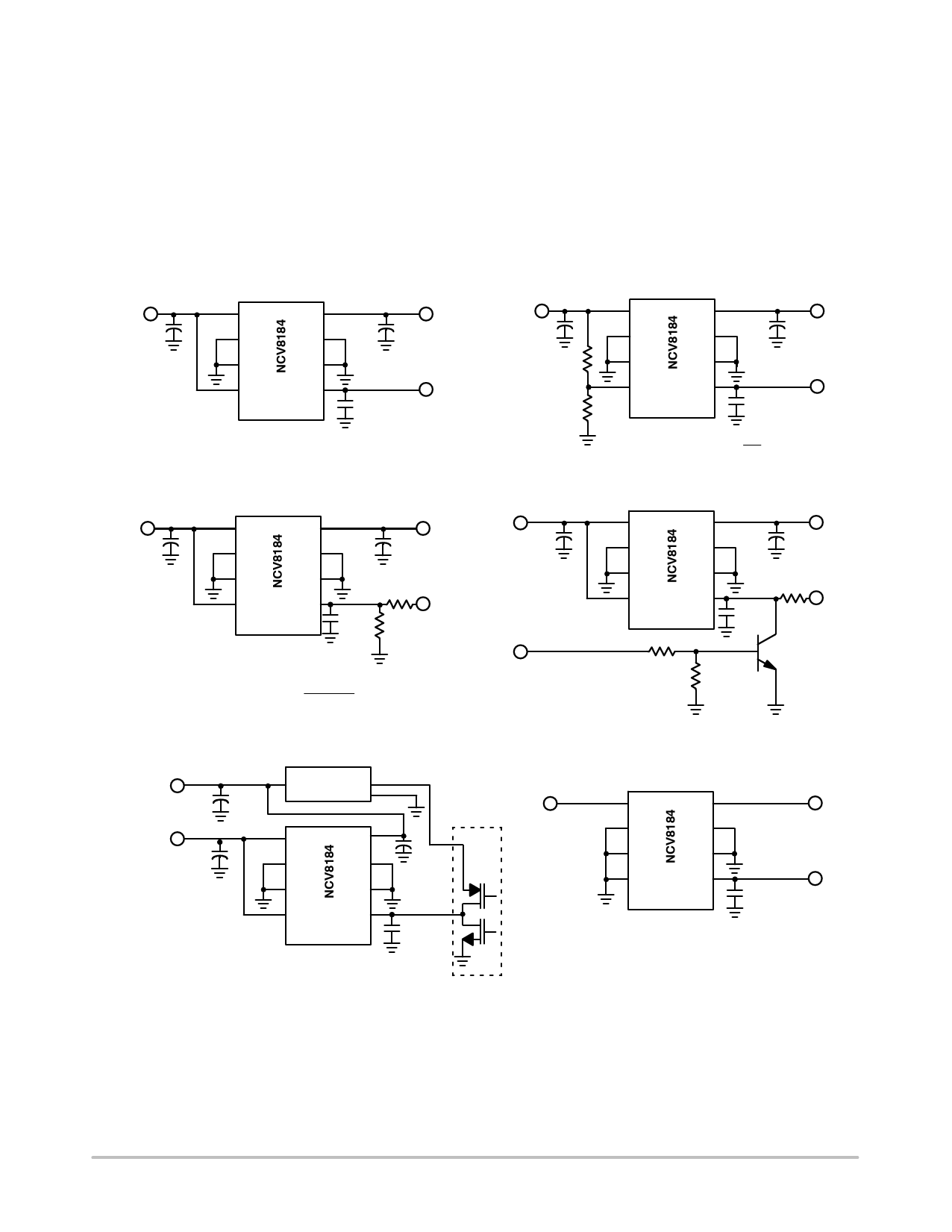
Loads VOUT, 70 mA
C2**
10 mF
VOUT
GND
VIN
GND
GND GND
Adj VREF/
ENABLE
VOUT + VREF
B+
C1*
1.0 mF
C3***
10 nF
5.0 V
Figure 13. Tracking Regulator at the Same Voltage
Loads VOUT, 70 mA
C2**
10 mF
RF
VOUT
GND
GND
VIN
GND
GND
B+
C1*
1.0 mF
RA
Adj VREF/
ENABLE
C3***
10 nF
VREF
VOUT + VREF(1 ) RREA)
Figure 14. Tracking Regulator at Higher Voltages
Loads VOUT, 70 mA
C2**
10 mF
VOUT
GND
VIN
GND
GND GND
Adj VREF/
ENABLE
B+
C1*
1.0 mF
R1
C3***
10 nF R2
VREF
VOUT, 70 mA VOUT
C2**
10 mF
GND
VIN
GND
GND GND
Adj VREF/
ENABLE
from MCU
B+
C1*
1.0 mF
R
C3***
10 nF
VREF
VOUT + VREF(R1R)2R2)
Figure 15. Tracking Regulator at Lower Voltages
Figure 16. Tracking Regulator with ENABLE Circuit
6.0 V−40 V
100 nF
70 mA
To Load 10 mF
(e.g. sensor)
VIN
NCV8501
VREF (5.0 V)
70 mA
VOUT
GND
VIN
GND
GND GND
Adj VREF/
ENABLE
C1*
mC
1.0 mF
I/O
C3***
10 nF
VOUT
VIN
GND GND
GND GND
Adj VREF/
ENABLE
C3***
10 nF
VOUT + B ) * VSAT
B+
MCU
Figure 17. Alternative ENABLE Circuit
Figure 18. High−Side Driver
* C1 is required if the regulator is far from the power source filter. In case of power supply generates voltage ripple (e.g. DC-DC con-
verter) a passive low pass filter with C1 value at least 1 mF is required to suppress the ripple. The filter should be designed according
to particular operating conditions and verified in the application.
** C2 is required for stability.
*** C3 is recommended for EMC susceptibility
http://onsemi.com
5
Share Link: 