ML7029 데이터 시트보기 (PDF) - LAPIS Semiconductor Co., Ltd.
부품명
상세내역
일치하는 목록
ML7029 Datasheet PDF : 29 Pages
| |||
FEDL7029-04
ML7029
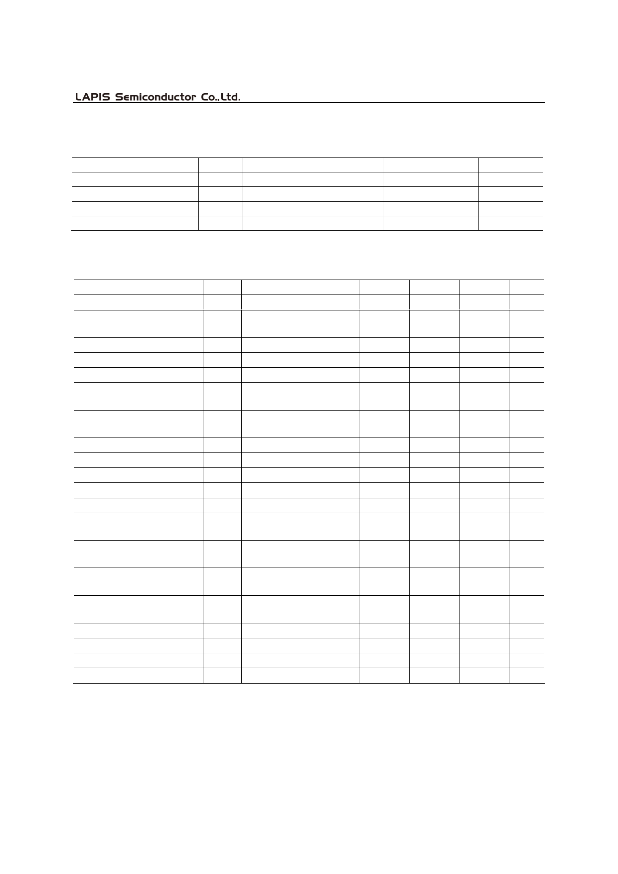
ABSOLUTE MAXIMUM RATINGS
Parameter
Power Supply Voltage
Analog Input Voltage
Digital Input Voltage
Storage Temperature
Symbol
VDD
VAIN
VDIN
Tstg
Condition
—
—
—
—
Rating
Unit
–.3 to +5.0
V
–0.3 to VDD+0.3
V
–0.3 to VDD+0.3
V
–55 to +150
C
RECOMMENDED OPERATION CONDITIONS
Parameter
Power Supply Voltage
Operating Temperature
Range
Digital Input High Voltage
Digital Input Low Voltage
Master Clock Frequency
Master Clock Frequency
Accuracy
Bit Clock Duty
Sampling Frequency (*1)
Master Clock Duty Ratio
Clock Duty Ratio
Digital Input Rise Time
Digital Input Fall Time
PCM Sync Signal Setting
Time (Continuous BCLK)
PCM Sync Signal Setting
Time (Burst Mode Clock)
SYNC Signal Width
(Continuous BCLK)
SYNC Signal Width
(Burst Mode Clock)
PCM, ADPCM Setup Time
PCM, ADPCM Hold Time
Digital Output Load
Bypass Capacitors for SG
*1: Refer to the Appendix.
Symbol
VDD
Ta
VIH
VIL
fMCK1
fMCK2
fBCK
fSYNC
DMCK
DCLK
tir
tif
tBS
tSB
tWS
tWSB
tDS
tDH
CDL
CSG
Condition
Voltage must be fixed
—
Digital Input Pins
Digital Input Pins
MCK
MCK
BCLK
SYNC
MCK(20.736 MHz)
BCLK, EXCK
Digital Input Pins
Digital Input Pins
BCLKSYNC
(see Fig. 3-1)
BCLK SYNC
(see Fig. 3-2)
SYNC (see Fig. 3-1)
SYNC (see Fig. 3-2)
—
—
Digital Output Pins
SG to AG
Min.
Typ.
Max.
Unit
+2.7
3.0
+3.6
V
–25
+25
+70
C
0.45 VDD
0
7.776
–0.01%
SYNC 8
6.0
30
30
—
—
—
VDD
—
0.16 VDD
10.368 20.736
SYNC
1296
+0.01%
—
SYNC
256
8.0
16
50
70
50
70
—
50
—
50
V
V
MHz
MHz
kHz
kHz
%
%
ns
ns
100
—
—
ns
0
1BCLK
1BCLK
100
100
—
10+0.1
—
20
s
—
SYNC –1
BCLK
s
—
Burst
Clock –1
s
—
—
ns
—
—
ns
—
100
pF
—
—
F
9/29
Share Link: 