ML7029 데이터 시트보기 (PDF) - LAPIS Semiconductor Co., Ltd.
부품명
상세내역
일치하는 목록
ML7029 Datasheet PDF : 29 Pages
| |||
FEDL7029-04
ML7029
DEN, EXCK, DIN, DOUT
Serial control ports for MCU interface.
Reading and writing data are performed by an external MCU through these pins. The 8-byte cotrol registers
(CR0 to 7) are provided on the device.
DEN is the “Enable” control signal input, EXCK is the data shift clock input, DIN is the address and data input,
and DOUT is the data output.
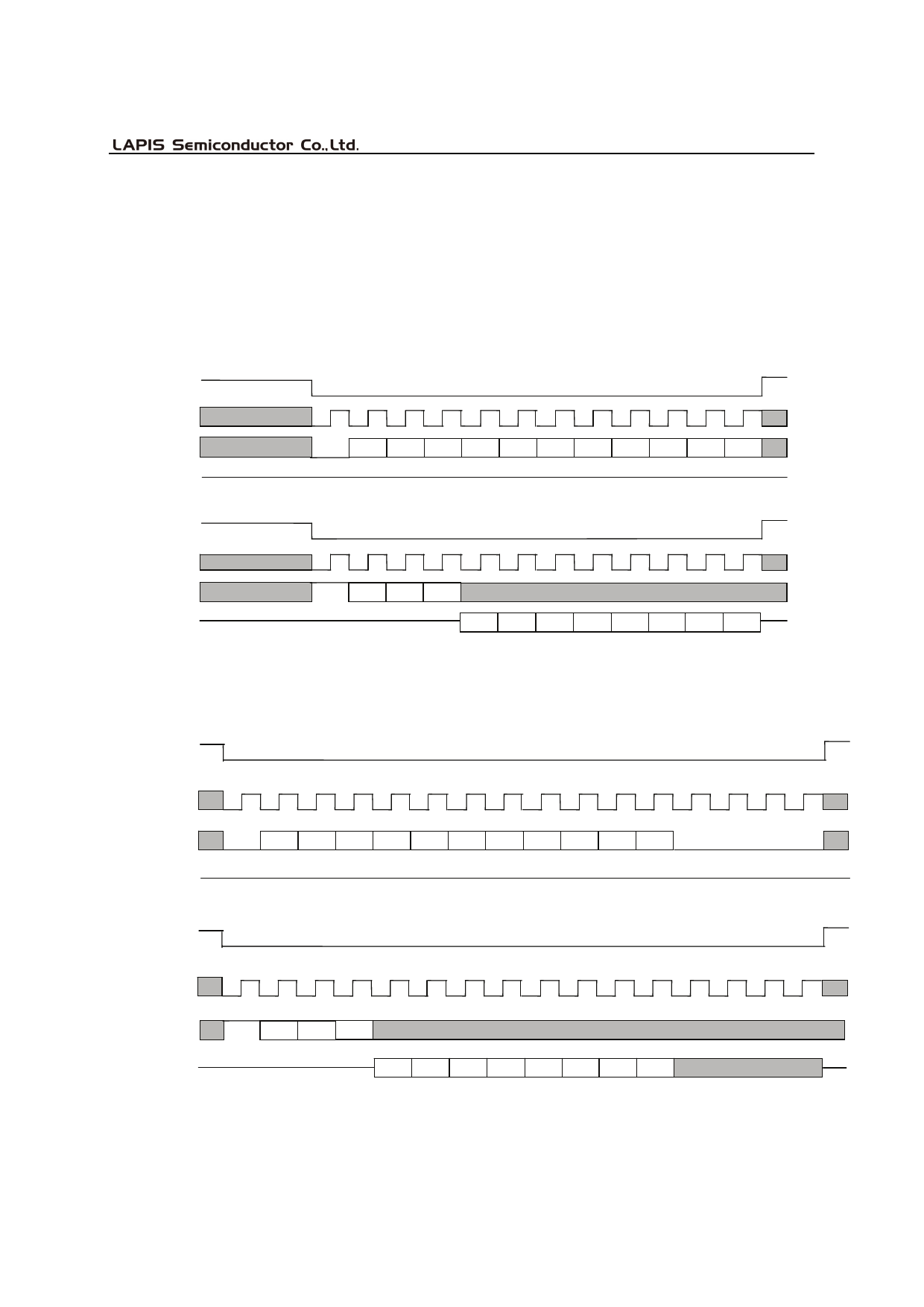
Figures 2-1 and 2-2 show the input/output timing diagram. During power-down, the DOUT output is in a high
impedance state.
DEN
EXCK
DIN
DOUT
DEN
EXCK
DIN
DOUT
W A2 A1 A0 B7 B6 B5 B4 B3 B2 B1 B0
High Impedance
(a) Data Write Timing Diagram
R A2 A1 A0
High Impedance
B7 B6 B5 B4 B3 B2 B1 B0
(b) Data Read Timing Diagram
Figure 2-1 MCU Interface Input/Output Timing (DIN = 12 bits)
DEN
EXCK
DIN
DOUT
DEN
EXCK
DIN
DOUT
W A2 A1 A0 B7 B6 B5 B4 B3 B2 B1 B0
High Impedance
(a) Data Write Timing Diagram
R A2 A1 A0
High Impedance
B7 B6 B5 B4 B3 B2 B1 B0
(b) Data Read Timing Diagram
Figure 2-2 MCU Interface Input/Output Timing (DIN = 16 bits)
7/29
Share Link: 