LLL216R71H103MD01K 데이터 시트보기 (PDF) - Unspecified
부품명
상세내역
일치하는 목록
LLL216R71H103MD01K Datasheet PDF : 296 Pages
| |||
!Note • Please read rating and !CAUTION (for storage, operating, rating, soldering, mounting and handling) in this catalog to prevent smoking and/or burning, etc.
• This catalog has only typical specifications. Therefore, please approve our product specifications or transact the approval sheet for product specifications before ordering.
Notice
Continued from the preceding page.
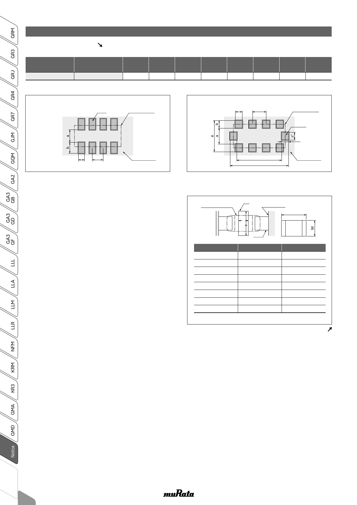
Table 5 LLM Series Reflow Soldering Method
Series
Chip Dimension Code Chip
(L/W)
(LgW)
LLM
21
2.0g1.25
a
b, b'
c, c'
0.6 to 0.8 (0.3 to 0.5)
0.3
b=(c-e)/2, b'=(d-f)/2
d
e
f
2.0 to 2.6 1.3 to 1.8 1.4 to 1.6
C02E.pdf
Nov.27,2017
p
0.5
(in mm)
[Land for LLA Series]
Land
Chip Capacitor
[Land for LLM Series]
c
p
Chip Capacitor
Land
b'
c
p
Solder Resist
f
Solder Resist
d
<Applicable to beyond Rated Voltage of 200VDC>
2-2. Dimensions of Slit (Example)
Preparing the slit helps flux cleaning and resin
coating on the back of the capacitor.
However, the length of the slit design should be as
short as possible to prevent mechanical damage in
the capacitor.
A longer slit design might receive more severe
mechanical stress from the PCB.
Recommended slit design is shown in the Table.
Chip Capacitor
LgW
1.6g0.8
2.0g1.25
3.2g1.6
3.2g2.5
4.5g2.0
4.5g3.2
5.7g2.8
5.7g5.0
Slit
Solder Resist
L
d
Land
d
–
–
1.0 to 2.0
1.0 to 2.0
1.0 to 2.8
1.0 to 2.8
1.0 to 4.0
1.0 to 4.0
e
–
–
3.2 to 3.7
4.1 to 4.6
3.6 to 4.1
4.8 to 5.3
4.4 to 4.9
6.6 to 7.1
(in mm)
Continued on the following page.
286
Share Link: 