LLL216R71H103MD01K 데이터 시트보기 (PDF) - Unspecified
부품명
상세내역
일치하는 목록
LLL216R71H103MD01K Datasheet PDF : 296 Pages
| |||
!Note • Please read rating and !CAUTION (for storage, operating, rating, soldering, mounting and handling) in this catalog to prevent smoking and/or burning, etc.
• This catalog has only typical specifications. Therefore, please approve our product specifications or transact the approval sheet for product specifications before ordering.
Notice
Continued from the preceding page.
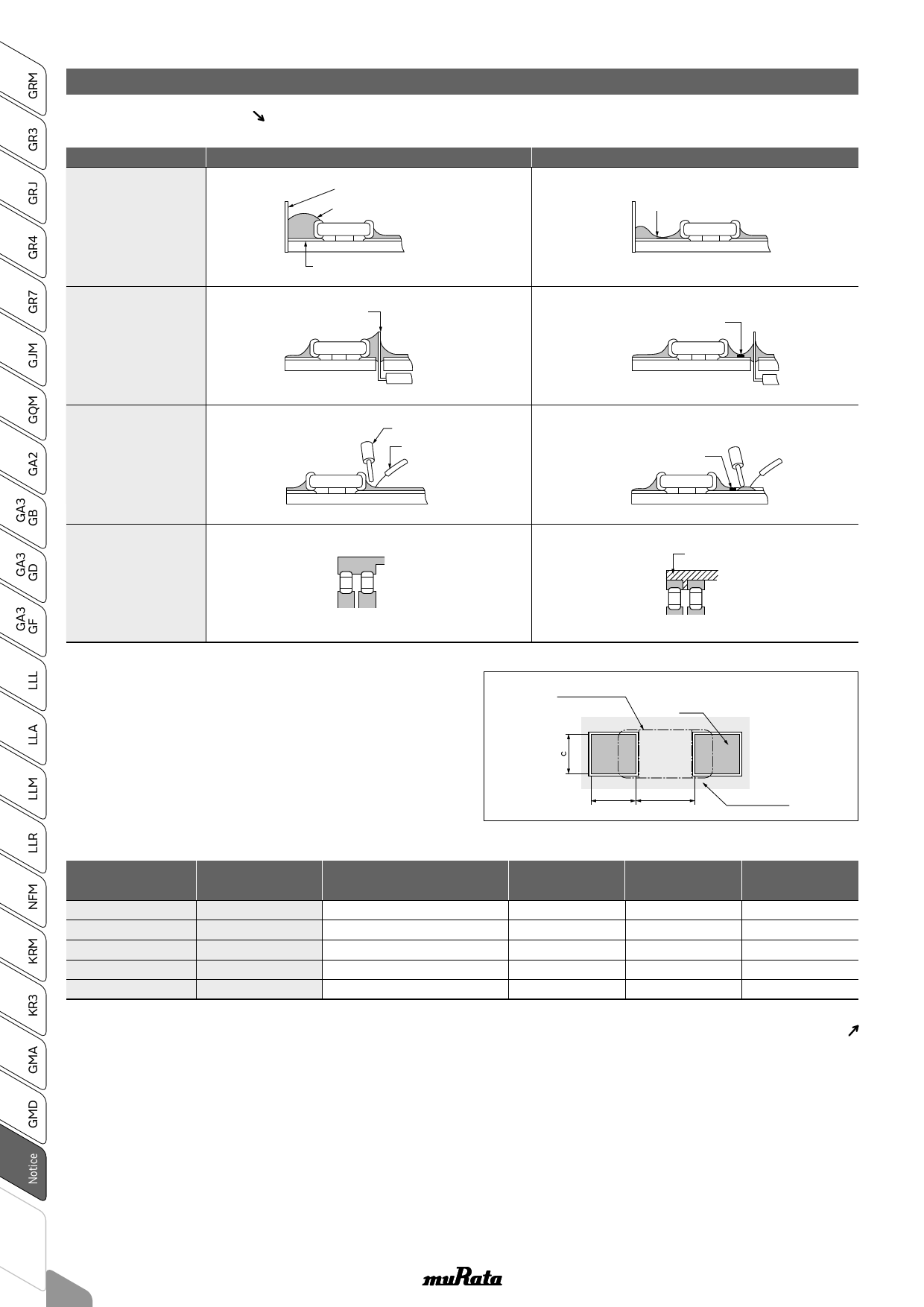
Pattern Forms
Placing Close to Chassis
Prohibited
Chassis
Solder (ground)
Correct
Solder Resist
Placing
of Chip Components
and Leaded Components
Placing
of Leaded Components
a er Chip Component
Lateral Mounting
Electrode Pattern
Lead Wire
in section
in section
Soldering Iron
Lead Wire
in section
Solder Resist
Solder Resist
Solder Resist
C02E.pdf
Nov.27,2017
in section
in section
in section
2. Land Dimensions
2-1. Please refer to the land dimensions in table 1 for flow
soldering, table 2 for reflow soldering, table 3 for
reflow soldering for ZRB Series, table 4 for reflow
soldering for LLA Series, table 5 for reflow soldering
for LLM Series.
Please confirm the suitable land dimension by
evaluating of the actual SET / PCB.
Table 1 Flow Soldering Method
Series
Chip Dimension Code
(L/W)
Chip (LgW)
GQM/GR3/GRJ/GRM 18
GQM/GR3/GRJ/GRM 21
GR3/GRJ/GRM
31
LLL
21
LLL
31
1.6g0.8
2.0g1.25
3.2g1.6
1.25g2.0
1.6g3.2
Flow soldering can only be used for products with a chip size from 1.6x0.8mm to 3.2x1.6mm.
Chip Capacitor
Land
b
a
Solder Resist
a
0.6 to 1.0
1.0 to 1.2
2.2 to 2.6
0.4 to 0.7
0.6 to 1.0
b
c
0.8 to 0.9
0.6 to 0.8
0.9 to 1.0
0.8 to 1.1
1.0 to 1.1
1.0 to 1.4
0.5 to 0.7
1.4 to 1.8
0.8 to 0.9
2.6 to 2.8
(in mm)
Continued on the following page.
284
Share Link: 