NCV51411(2019) 데이터 시트보기 (PDF) - ON Semiconductor
부품명
상세내역
일치하는 목록
NCV51411
(Rev.:2019)
(Rev.:2019)
ON Semiconductor

NCV51411 Datasheet PDF : 18 Pages
| |||
NCV51411
BOOST Pin
The BOOST pin provides base driving current for the
power switch. A voltage higher than VIN provides required
headroom to turn on the power switch. This in turn reduces
IC power dissipation and improves overall system
efficiency. The BOOST pin can be connected to an external
boost−strapping circuit which typically uses a 0.1 mF capacitor
and a 1N914 or 1N4148 diode, as shown in Figure 1. When the
power switch is turned on, the voltage on the BOOST pin is
equal to
VBOOST + VIN ) VO * VF
where:
VF = diode forward voltage.
The anode of the diode can be connected to any DC
voltage as well as the regulated output voltage (Figure 1).
However, the maximum voltage on the BOOST pin shall not
exceed 40 V.
As shown in Figure 7, the BOOST pin current includes a
constant 7.0 mA pre−driver current and base current
proportional to switch conducting current. A detailed
discussion of this current is conducted in Thermal
Consideration section. A 0.1 mF capacitor is usually
adequate for maintaining the Boost pin voltage during the on
time.
30
25
20
15
10
5
00
0.5
1.0
1.5
SWITCHING CURRENT (A)
Figure 7. The Boost Pin Current Includes 7.0 mA
Pre−Driver Current and Base Current when the
Switch is Turned On. The Beta Decline of the
Power Switch Further Increases the Base
Current at High Switching Current
Shutdown
The internal power switch will not turn on until the VIN
pin rises above the Startup Voltage. This ensures no
switching until adequate supply voltage is provided to the
IC. The IC transitions to sleep mode when the SHDNB pin
is pulled low. In sleep mode, the internal power switch
transistor remains off and supply current is reduced to the
Shutdown Quiescent Current value (20 mA typical). This pin
has an internal pull-up current source, so defaults to high
(enabled) state when not connected.
VIN
I1
5mA
Q2
To internal
bias rails
SHDNB
(a)
20k
Q1
D1
8V
0.65V
SHDNB
Z1
(b)
2V to 5V
(c)
SHDNB
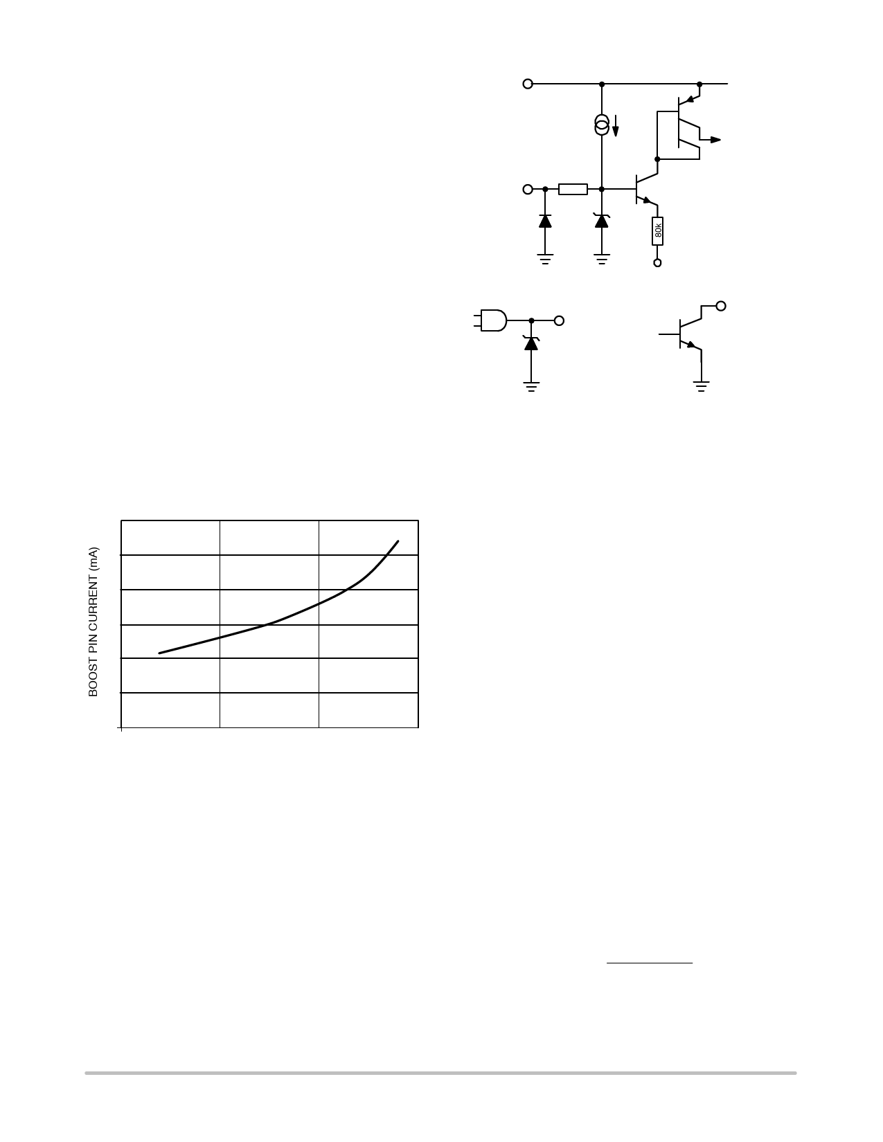
Figure 8. SHDNB pin equivalent internal circuit (a)
and practical interface examples (b), (c).
Figure 8(a) depicts the SHDNB pin equivalent internal
circuit. If the pin is open, current source I1 flows into the
base of Q1, turning both Q1 and Q2 on. In turn, Q2 collector
current enables the various internal power rails. In
Figure 8(b), a standard logic gate is used to pull the pin low
by shunting I1 to ground, which places the IC in sleep
(shutdown) mode. Note that, when the gate output is logical
high, the voltage at the SHDNB pin will rise to the internal
clamp voltage of 8 V. This level exceeds the maximum
output rating for most common logic families. Protection
Zener diode Z1 permits the pin voltage to rise high enough
to enable the IC, but remain less than the gate output voltage
rating. In Figure 8(c), a single open-collector general-
purpose NPN transistor is used to pull the pin low. Since
transistors generally have a maximum collector voltage
rating in excess of 8 V, the protection Zener diode in
Figure 8(b) is not required.
Startup
During power up, the regulator tends to quickly charge up
the output capacitors to reach voltage regulation. This gives
rise to an excessive in−rush current which can be detrimental
to the inductor, IC and catch diode. In V2 control , the
compensation capacitor provides Soft−Start with no need
for extra pin or circuitry. During the power up, the Output
Source Current of the error amplifier charges the
compensation capacitor which forces VC pin and thus output
voltage ramp up gradually. The Soft−Start duration can be
calculated by
TSS
+
VC CCOMP
ISOURCE
where:
VC = VC pin steady−state voltage, which is approximately
equal to error amplifier’s reference voltage.
http://onsemi.com
8
Share Link: