NCV51411(2019) 데이터 시트보기 (PDF) - ON Semiconductor
부품명
상세내역
일치하는 목록
NCV51411
(Rev.:2019)
(Rev.:2019)
ON Semiconductor

NCV51411 Datasheet PDF : 18 Pages
| |||
NCV51411
PACKAGE PIN DESCRIPTION
SO−8 SO−16 DFN−18 PIN SYMBOL
FUNCTION
1
15
1
BOOST
The BOOST pin provides additional drive voltage to the on−chip NPN power transist-
or. The resulting decrease in switch on voltage increases efficiency.
2
16
2, 3, 4
3
1
5, 6, 7
VIN
This pin is the main power input to the IC.
VSW
This is the connection to the emitter of the on−chip NPN power transistor and serves
as the switch output to the inductor. This pin may be subjected to negative voltages
during switch off−time. A catch diode is required to clamp the pin voltage in normal
operation. This node can stand −1.0 V for less than 50 ns during switch node flyback.
4
2
8
SHDNB
Shutdown_bar input. This is an active−low logical input, TTL compatible, with an in-
ternal pull−up current source. The IC goes into sleep mode, drawing less than 85 mA
when the pin voltage is pulled below 1.0 V. This pin may be left floating in applications
where a shutdown function is not required.
5
7
10
SYNC
This pin provides the synchronization input.
6
8
13
GND
Power return connection for the IC.
7
9
16
VFB
The FB pin provides input to the inverting input of the error amplifier. If VFB is lower
than 0.29 V, the oscillator frequency is divided by four, and current limit folds back to
about 1 ampere. These features protect the IC under severe overcurrent or short cir-
cuit conditions.
8
10
17
VC
The VC pin provides a connection point to the output of the error amplifier and input to
the PWM comparator. Driving of this pin should be avoided because on−chip test
circuitry becomes active whenever current exceeding 0.5 mA is forced into the IC.
−
3 − 6, 9, 11, 12,
11 − 14 14, 15, 18
NC
No Connection
1
BOOST
VIN
VSW
SHDNB
8
VC
VFB
GND
SYNC
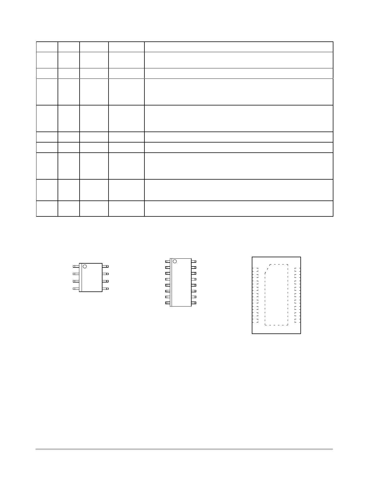
SO−8
PIN CONNECTIONS
1
VSW
SHDNB
NC
NC
NC
NC
SYNC
GND
16
VIN
BOOST
NC
NC
NC
NC
VC
VFB
SO−16W EP
BOOST 1
VIN
2
VIN
3
VIN
4
Vsw 5
VSW
6
VSW
7
SHDNB 8
NC 9
18 NC
17 VC
16
VFB
15 NC
14 NC
13 GND
12 NC
11 NC
10 SYNC
18−Lead DFN
Note: DFN exposed pad may be soldered to a
heat spreader for enhanced thermal perform-
ance. The exposed pad may be connected to
GND; do not connect to any other potential.
http://onsemi.com
3
Share Link: