NCV51411(2019) 데이터 시트보기 (PDF) - ON Semiconductor
부품명
상세내역
일치하는 목록
NCV51411
(Rev.:2019)
(Rev.:2019)
ON Semiconductor

NCV51411 Datasheet PDF : 18 Pages
| |||
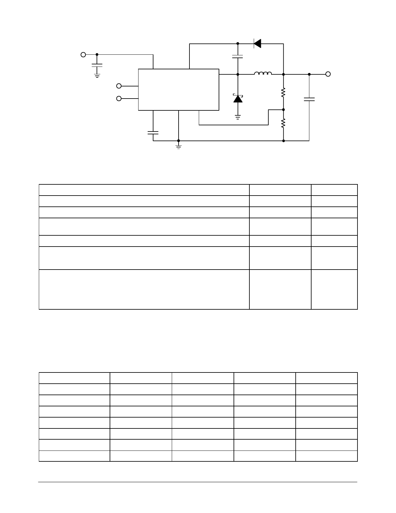
NCV51411
4.5 V − 16 V
C2
100 mF
Shutdown
SYNC
U1 2
VIN
4
SHDNB
5
SYNC
VC
8
1
BOOST
3
VSW
NCV51411
GND VFB
6
7
C4
0.1 mF
D1 1N4148
C1
0.1 mF
L1
15 mH
R1
D3
205
1N5821
R2
127
3.3 V
C3
100 mF
Figure 1. Application Diagram, 4.5 V − 16 V to 3.3 V @ 1.0 A Converter
MAXIMUM RATINGS*
Rating
Value
Unit
Peak Transient Voltage (31 V Load Dump @ VIN = 14 V)
45
V
Operating Junction Temperature Range, TJ
−40 to 150
°C
Lead Temperature Soldering:
Reflow: (Note 1)
240 peak
°C
(Note 2)
Storage Temperature Range, TS
ESD
−65 to +150
°C
(Human Body Model)
2.0
kV
(Machine Model)
200
V
(Charge Device Model)
>1.0
kV
Package Thermal Resistance
SO−8 Junction−to−Case, RqJC
45
SO−8 Junction−to−Ambient, RqJA
165
SO−16 Junction−to−Case, RqJC
16
SO−16 Junction−to−Ambient, RqJA (Note 3)
35
18−Lead DFN Junction−to−Ambient, RqJA (Note 3)
38
°C/W
°C/W
°C/W
°C/W
°C/W
Stresses exceeding Maximum Ratings may damage the device. Maximum Ratings are stress ratings only. Functional operation above the
Recommended Operating Conditions is not implied. Extended exposure to stresses above the Recommended Operating Conditions may affect
device reliability.
*The maximum package power dissipation must be observed.
1. 60 second maximum above 183°C.
2. −5°C/0°C allowable conditions.
3. 4 layer board, 1 oz copper outer layers, 0.5 oz copper inner layers, 600 sqmm copper area
MAXIMUM RATINGS (Voltages are with respect to GND)
Pin Name
VIN (DC)*
BOOST
VMax
40 V
40 V
VMIN
−0.3 V
−0.3 V
VSW
VC
SHDNB
40 V
7.0 V
7.0 V
−0.6 V/−1.0 V, t < 50 ns
−0.3 V
−0.3 V
SYNC
7.0 V
−0.3 V
VFB
*See table above for load dump.
7.0 V
−0.3 V
ISOURCE
N/A
N/A
4.0 A
1.0 mA
1.0 mA
1.0 mA
1.0 mA
ISINK
4.0 A
100 mA
10 mA
1.0 mA
1.0 mA
1.0 mA
1.0 mA
http://onsemi.com
2
Share Link: