74LV595 데이터 시트보기 (PDF) - NXP Semiconductors.
부품명
상세내역
일치하는 목록
74LV595 Datasheet PDF : 20 Pages
| |||
NXP Semiconductors
74LV595
8-bit serial-in/serial-out or parallel-out shift register; 3-state
VI
SHCP input
GND
VI
STCP input
GND
VOH
Qn output
VOL
VM
t su
VM
tW
t PLH
VM
1/ fmax
t PHL
mna558
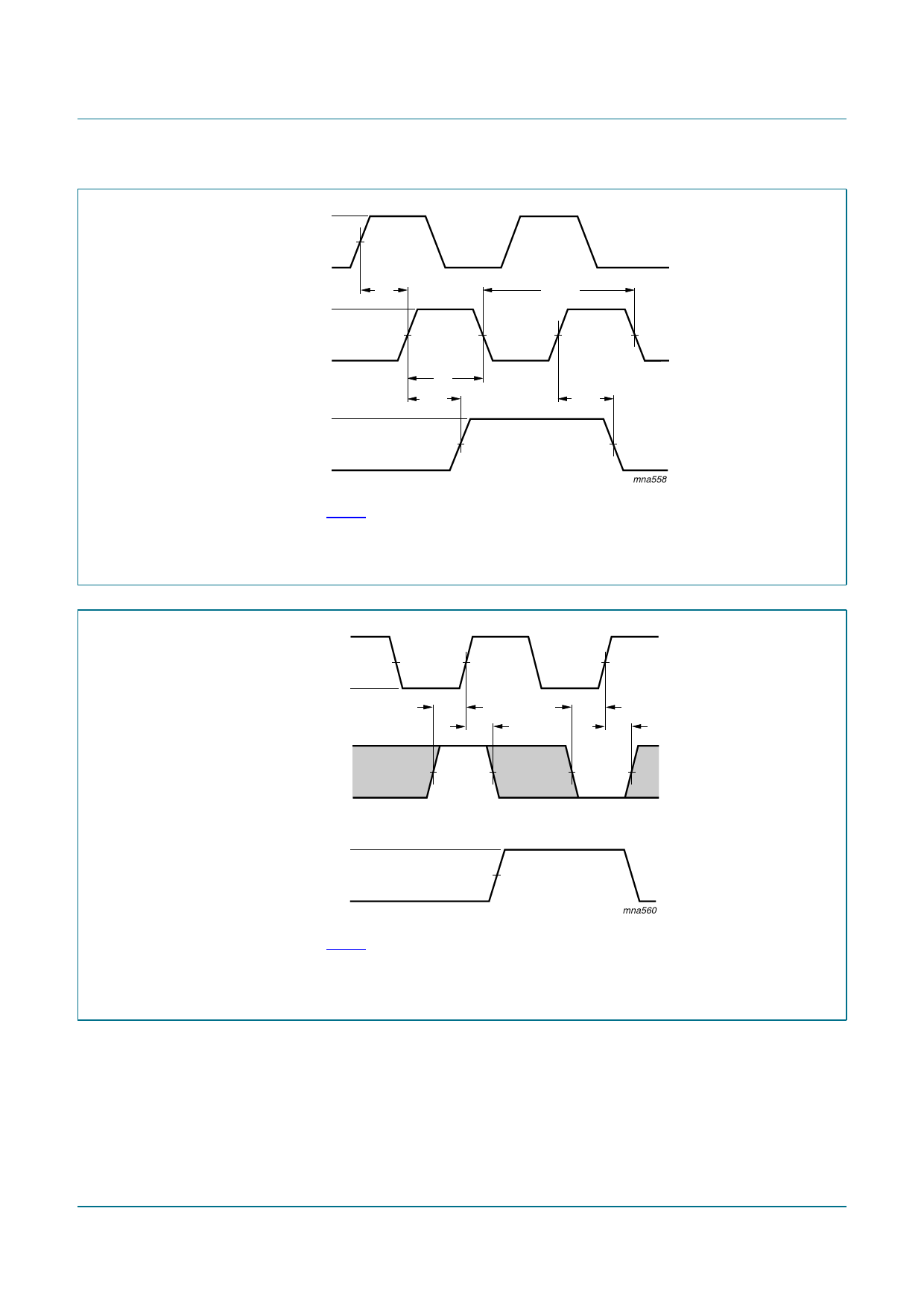
Fig 9.
Measurement points are given in Table 8.
VOL and VOH are typical output voltage drops that occur with the output load.
The storage clock (STCP) to parallel data output (Qn) propagation delays, the storage clock pulse width
and the shift clock to storage clock set-up time
VI
SHCP input
GND
VI
DS input
GND
VM
t su
th
VM
t su
th
VOH
Q7S output
VOL
VM
mna560
Measurement points are given in Table 8.
The shaded areas indicate when the input is permitted to change for predictable output performance.
VOL and VOH are typical output voltage drops that occur with the output load.
Fig 10. The data set-up and hold times for the serial data input (DS)
74LV595_3
Product data sheet
Rev. 03 — 21 April 2009
© NXP B.V. 2009. All rights reserved.
11 of 20
Share Link: 