MM908E625 데이터 시트보기 (PDF) - Freescale Semiconductor
부품명
상세내역
일치하는 목록
MM908E625
Freescale Semiconductor

MM908E625 Datasheet PDF : 49 Pages
| |||
ELECTRICAL CHARACTERISTICS
MAXIMUM RATINGS
ELECTRICAL CHARACTERISTICS
MAXIMUM RATINGS
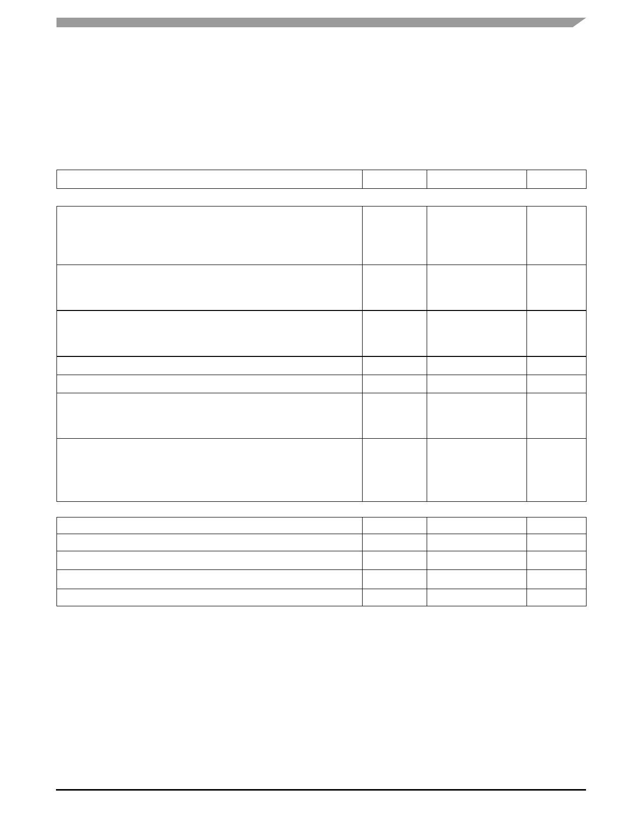
Table 2. Maximum Ratings
All voltages are with respect to ground unless otherwise noted. Exceeding these ratings may cause a malfunction or
permanent damage to the device.
Ratings
Symbol
Value
Unit
ELECTRICAL RATINGS
Supply Voltage
Analog Chip Supply Voltage under Normal Operation, Steady State
Analog Chip Supply Voltage under Transient Conditions (1)
Microcontroller Chip Supply Voltage
Input Pin Voltage
Analog Chip
Microcontroller Chip
Maximum Microcontroller Current per Pin
All Pins Except VDD, VSS, PTA0:PTA6, PTC0:PTC1
Pins PTA0:PTA6, PTC0:PTC1
Maximum Microcontroller VSS Output Current
Maximum Microcontroller VDD Input Current
LIN Supply Voltage
Normal Operation (Steady-State)
Transient Conditions (1)
ESD Voltage
Human Body Model (HBM)(2)
Machine Model (MM)(3)
Charge Device Model (CDM)(4)
V
VSUP(SS)
-0.3 to 28
VSUP(PK)
-0.3 to 40
VDD
-0.3 to 6.0
V
VIN (ANALOG)
VIN (MCU)
-0.3 to 5.5
VSS-0.3 to VDD+0.3
mA
IPIN(1)
±15
IPIN(2)
± 25
IMVSS
100
mA
IMVDD
100
mA
V
VBUS(SS)
VBUS(DYNAMIC)
-18 to 28
40
V
VESD
± 3000
± 150
± 500
THERMAL RATINGS
Storage Temperature
Ambient Operating Temperature
Operating Case Temperature (5)
TSTG
-40 to 150
°C
TA
-40 to 85
°C
TC
-40 to 85
°C
Operating Junction Temperature(6)
Peak Package Reflow Temperature During Reflow(7)(8)
TJ
-40 to 125
°C
TPPRT
Note 8
°C
Notes
1. Transient capability for pulses with a time of t < 0.5 sec.
2. ESD voltage testing is performed in accordance with the Human Body Model (CZAP = 100 pF, RZAP = 1500 Ω)
3. ESD voltage testing is performed in accordance with the Machine Model (CZAP =200 pF, RZAP = 0 Ω)
4. ESD voltage testing is performed in accordance with Charge Device Model, robotic (CZAP =4.0 pF).
5. The limiting factor is junction temperature, taking into account the power dissipation, thermal resistance, and heat sinking.
6. The temperature of analog and MCU die is strongly linked via the package, but can differ in dynamic load conditions, usually because
of higher power dissipation on the analog die. The analog die temperature must not exceed 150 °C under these conditions.
7. Pin soldering temperature is for 10 seconds maximum duration. Not designed for immersion soldering. Exceeding these limits may cause
malfunction or permanent damage to the device.
8. Freescale’s Package Reflow capability meets Pb-free requirements for JEDEC standard J-STD-020C. For Peak Package Reflow
Temperature and Moisture Sensitivity Levels (MSL), Go to www.freescale.com, search by part number [e.g. remove prefixes/suffixes
and enter the core ID to view all orderable parts. (i.e. MC33xxxD enter 33xxx), and review parametrics.
Analog Integrated Circuit Device Data
Freescale Semiconductor
908E625
5
Share Link: