CS5231-3 데이터 시트보기 (PDF) - Cherry semiconductor
부품명
상세내역
일치하는 목록
CS5231-3 Datasheet PDF : 11 Pages
| |||
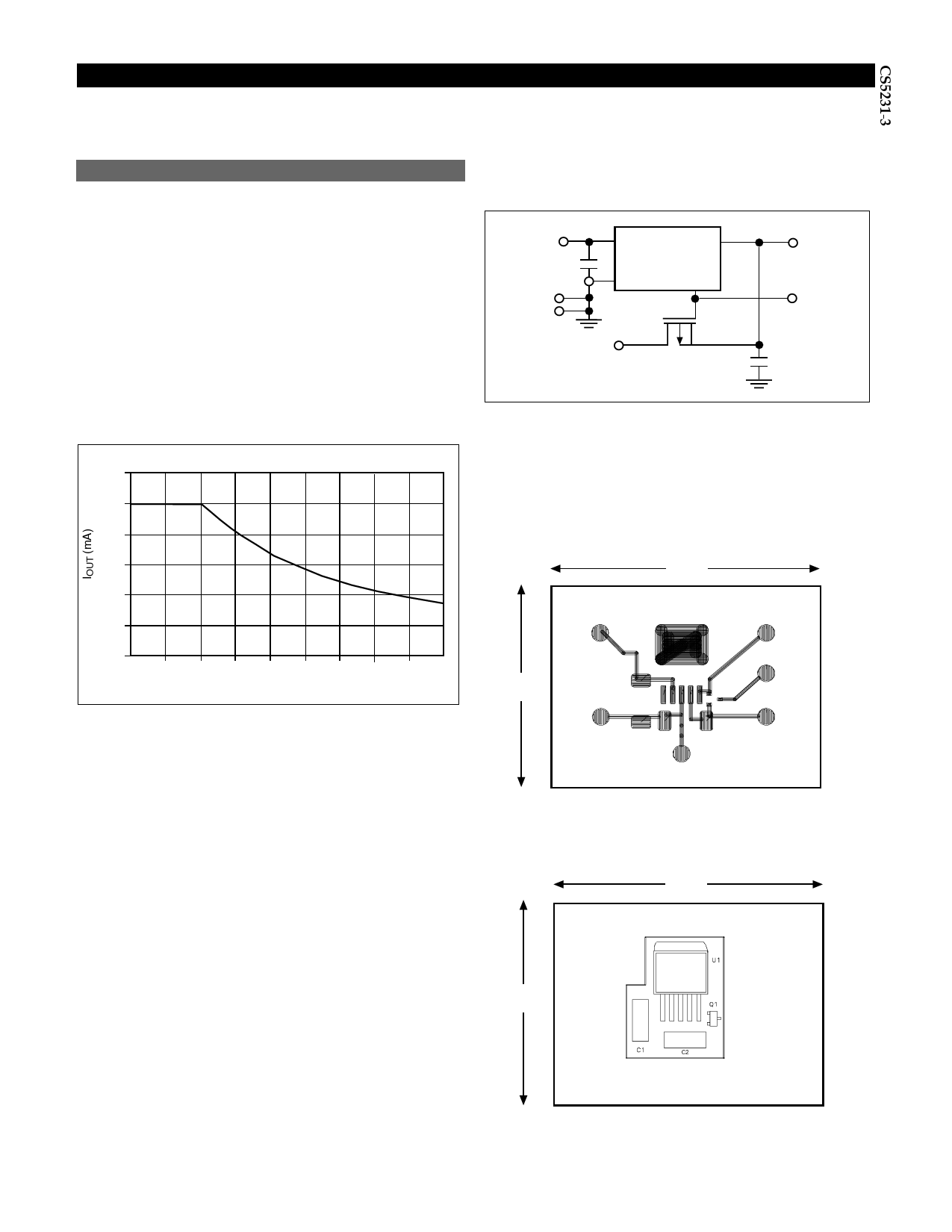
Application Circuit Characteristics
PC board by soldering both tab and leads will provide
superior performance with no PC board area penalty.
Description
The CS5231-3 application circuit has been implemented as
shown in the following pages. The schematic, bill of mate-
rials and printed circuit board artwork can be used to build
the circuit. The design is very simple and consists of two
capacitors, a p-channel FET and the CS5231-3. Five turret
pins are provided for connection of supplies, meters, oscil-
loscope probes and loads. The CS5231-3 power supply
management solution is implemented in an area less than
1.5 square inches. Due to the simplicity of the design, out-
put current must be derated if the CS5231-3 is operated at
VIN voltages greater than 7V. Figure 15 provides the derat-
ing curve on a maximum power dissipation if heatsink is
added. Operating at higher power dissipation without
heatsink may result in a thermal shutdown condition.
The VOUT Connection
The VOUT connection is tied to the VOUT lead of the
CS5231-3 and the PFET source. This point provides a con-
venient point at which some type of lead may be applied.
VIN TP1
C1
GND
TP2
TP3
U1
VIN
VOUT
CS5231-3
GND AUXDRV
Q1
TP4
+3.3V VAUX
C2
TP5
TP6
AUXDRV
Application Circuit Schematic
600
500
400
300
200
100
0
5 6 7 8 9 10 11 12 13 14
VIN(VOLTS)
Figure 6: Demo Board Output Current Derating vs VIN
PC Board Layout Artwork
The PC board is a single layer copper design. The layout
artwork is reproduced at actual size below.
2"
1.5"
The VIN Connection
The VIN connection is denoted as such on the PC board.
The maximum input voltage to the IC is 14V before dam-
age to the IC is possible. However, the specification range
for the IC is 4.75V < VIN < 6V.
The Gnd Connection
The Gnd connection ties the IC power return to two turret
pins. The extra turret pin provides for connection of multi-
ple instrument grounds to the demonstration board.
The AuxDrv Connection
The AuxDrv lead of the CS5231-3 is connected to the gate
of the external PFET. This connection is also brought to a
turret pin to allow easy connection of an oscilloscope probe
for viewing the AuxDrv waveforms.
The VAUX Connection
The VAUX turret pin provides a connection point between
an external 3.3V supply and the PFET drain.
Top Copper Layer
VIN 5V
1.5"
GND
2"
AUX.DRV
AUX3.3V
VOUT 3.3V
GND
Top Silk Screen Layer
9
Share Link: 