CS5231-3 데이터 시트보기 (PDF) - Cherry semiconductor
부품명
상세내역
일치하는 목록
CS5231-3 Datasheet PDF : 11 Pages
| |||
Application Information: continued
cally 25°C and allows the IC to recover from a thermal
fault without the need for an external reset signal. The
monitoring circuitry is located near the composite PNP-
NPN output transistor, since this transistor is responsible
for most of the on-chip power dissipation. The combina-
tion of current limit and thermal shutdown will protect the
IC from nearly any fault condition.
Reverse Current Protection
During normal system operation, the auxiliary drive cir-
cuitry will maintain voltage on the VOUT pin when VIN is
absent. IC reliability and system efficiency are improved
by limiting the amount of reverse current that flows from
VOUT to ground and from VOUT to VIN. Current flows from
VOUT to ground through the feedback resistor divider that
sets up the output voltage. This resistor can range in value
from 6kΩ to about 10kΩ, and roughly 500µA will flow in
the typical case. Current flow from VOUT to VIN will be
limited to leakage current after the IC shuts down. On-chip
RC time constants are such that the output transistor
should be turned off well before VIN drops below the VOUT
voltage.
and heatsink-to-air thermal resistance (θSA). The resulting
equation for junction-to-air thermal resistance is
θJA = θJC + θCS + θSA
The value of θJC for the CS5231-3 is provided in the
Packaging Information section of this data sheet. θCS can
be considered zero, since heat is conducted out of the
package by the IC leads and the tab of the D2PAK package,
and since the IC leads and tab are soldered directly to the
PC board.
Modification of θSA is the primary means of thermal man-
agement. For surface mount components, this means mod-
ifying the amount of trace metal that connects to the IC.
The thermal capacity of PC board traces is dependent on
how much copper area is used, whether or not the IC is in
direct contact with the metal, whether or not the metal sur-
face is coated with some type of sealant, and whether or
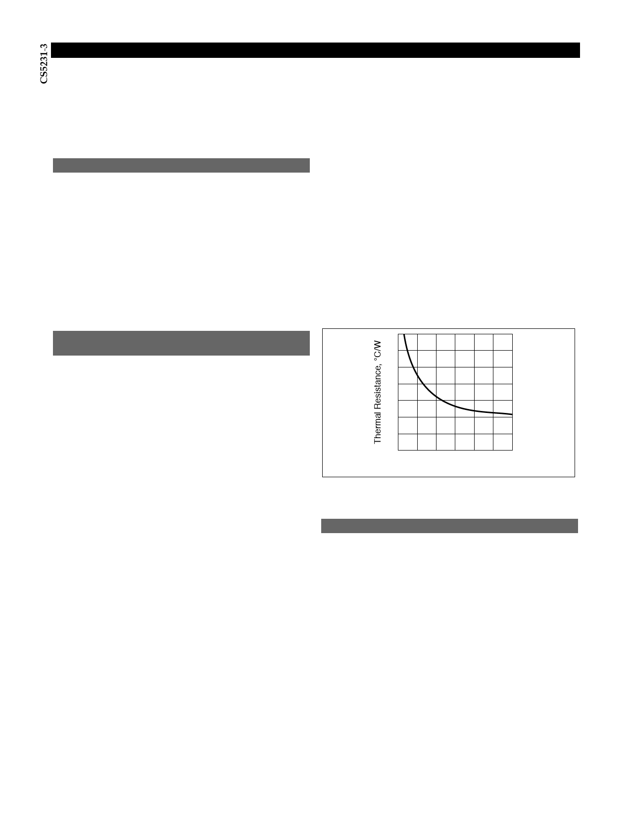
not there is airflow across the PC board. The chart provid-
ed below shows heatsinking capability of a square, single
sided copper PC board trace. The area is given in square
millimeters. It is assumed there is no airflow across the PC
board.
Calculating Power Dissipation and
Heatsink Requirements
Most linear regulators operate under conditions that result
in high on-chip power dissipation. This results in high
junction temperatures. Since the IC has a thermal shut-
down feature, ensuring the regulator will operate correctly
under normal conditions is an important design considera-
tion. Some heatsinking will usually be required.
Thermal characteristics of an IC depend on four parame-
ters: ambient temperature (TA in °C), power dissipation
(PD in watts), thermal resistance from the die to the ambi-
ent air (θJA in °C per watt) and junction temperature (TJ in
°C). The maximum junction temperature is calculated from
the formula below:
TJ(MAX) = TA(MAX) + (θJA) (PD(MAX))
Maximum ambient temperature and power dissipation are
determined by the design, while θJA is dependent on the
package manufacturer. The maximum junction tempera-
ture for operation of the CS5231-3 within specification is
150°C. The maximum power dissipation of a linear regula-
tor is given as
PD(MAX) = (Vin(MAX) − VOUT(MIN)) (ILOAD(MAX))
+ (VIN (MAX)) (IGnd(MAX))
where IGnd(MAX) is the IC bias current.
It is possible to change the effective value of θJA by adding
a heatsink to the design. A heatsink serves in some manner
to raise the effective area of the package, thus improving
the flow of heat from the package into the surrounding air.
Each material in the path of heat flow has its own charac-
teristic thermal resistance, all measured in °C per watt. The
thermal resistances are summed to determine the total
thermal resistance between the die junction and air. There
are three components of interest: junction-to-case thermal
resistance (θJC), case-to-heatsink thermal resistance (θCS)
70
60
50
40
30
20
10
00
2000
4000
6000
PC Board Trace Area (mm2)
Figure 5: Thermal Resistance Capability of Copper PC Board Metal
Traces
Typical D2PAK PC Board Heatsink Design
A typical design of the PC board surface area needed for
the D2PAK package is shown below. Calculations were
made assuming VIN(MAX) =5.25V, VOUT(MIN) = 3.266V,
IOUT(MAX) = 500mA, IGnd(MAX) = 5mA and TA = 70°C.
PD = (5.25V − 3.266V) (0.5A) + (5.25V) (0.005A) = 1018mW
Maximum temperature rise ∆T = TJ(MAX) − TA =
150°C − 70°C = 80°C.
θJA (worst case) = ∆T/PD = 80°C/1.018W = 78.56°C/W
First, we determine the need for heatsinking. If we assume
the maximum θJA = 50°C/W for the D2PAK, the maximum
temperature rise is found to be
∆T = (PD) (θJA) = (1.018W) (50°C/W) = 50.9°C
This is less than the maximum specified operating junction
temperature of 125°C, and no heatsinking is required.
Since the D2PAK has a large tab, mounting this part to the
8
Share Link: 