CS5231-3 데이터 시트보기 (PDF) - Cherry semiconductor
부품명
상세내역
일치하는 목록
CS5231-3 Datasheet PDF : 11 Pages
| |||
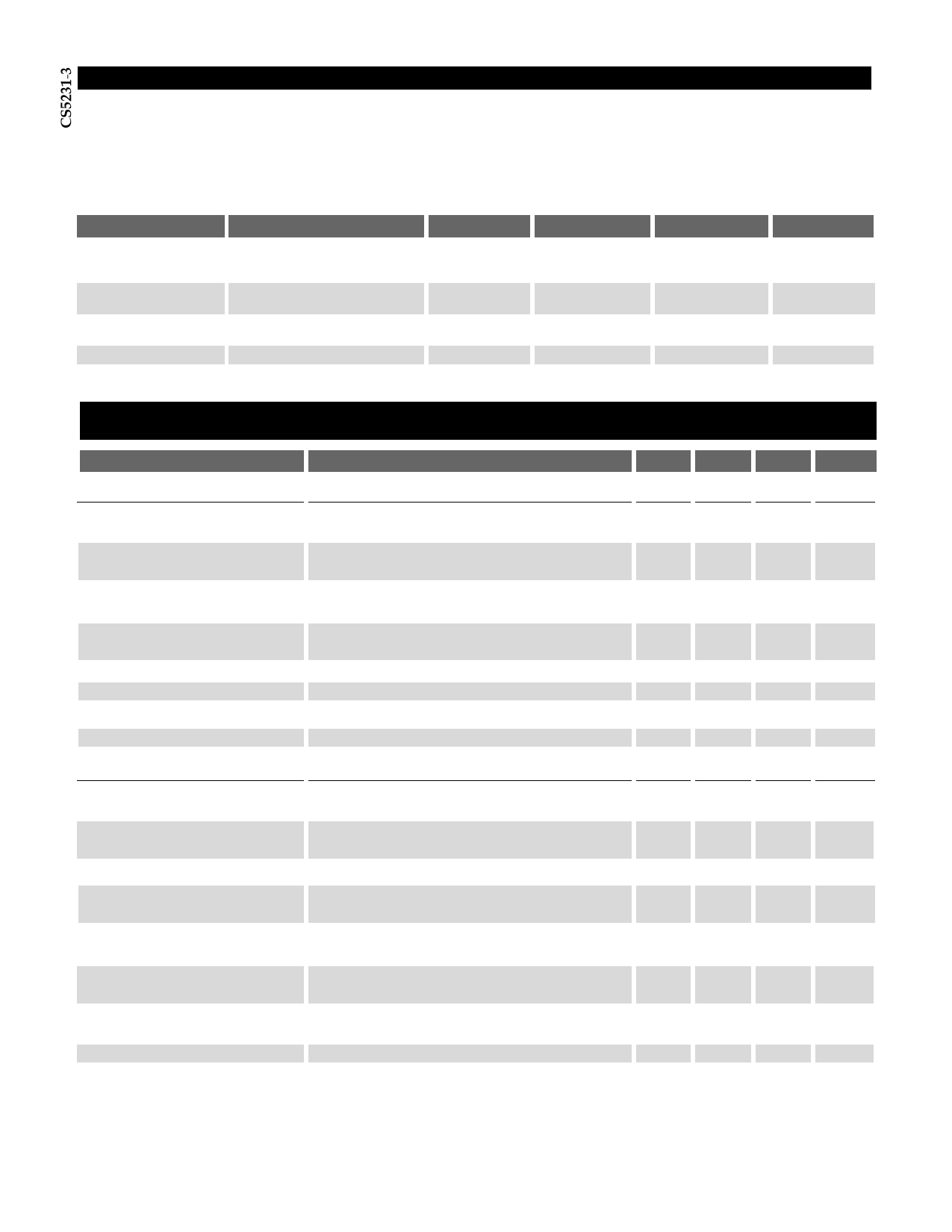
Absolute Maximum Ratings
Maximum Operating Junction Temperature ..........................................................................................................................150°C
Storage Temperature Range .....................................................................................................................................-65°C to +150°C
Lead Temperature Soldering
Reflow (SMD styles only) ...........................................................................................60 sec. max above 183°C, 230°C peak
ESD Damage Threshold (Human Body Model)....................................................................................................................2kV
PIN SYMBOL
VIN
VOUT
AuxDrv
Gnd
PIN NAME
IC Power Input
Output Voltage
Auxiliary Drive Output
IC Ground
VMAX
14V
6V
14V
N/A
VMIN
-0.3V
-0.3V
-0.3V
N/A
ISOURCE
100mA
Internally
Limited
10mA
N/A
ISINK
Internally
Limited
100mA
50mA
N/A
Electrical Characteristics: 0°C < TA < 70°C, 0°C < TJ < 125°C, 4.75V ≤ VCC < 6V, COUT ≥ 10µF with ESR < 1Ω,
IOUT = 10mA, unless otherwise specified.
PARAMETER
s Linear Regulator
Output Voltage
TEST CONDITIONS
10mA < IOUT < 500mA
Line Regulation
Load Regulation
Ground Current
Reverse Current
Current Limit
Thermal Shutdown
Thermal Shutdown Hysteresis
s Auxiliary Drive
Upper VIN Threshold
Lower VIN Threshold
VIN Threshold Hysteresis
Output Low Voltage
Output Low Peak Voltage
AuxDrv Current Limit
Response Time
Pull-Up/Down Resistance
IOUT = 10mA,
VIN = 4.75V to 6V
VIN = 5V,
IOUT = 10mA to 500mA
IOUT = 10mA
IOUT = 500mA
VIN = 0V, VOUT = 3.3V
0V < VOUT < 3.2V
Note 1
Note 1
Increase VIN until regulator turns on
and AuxDrv drives high
Decrease VIN until regulator turns off
and AuxDrv drives low
IAuxDrv = 100µA,
1V < VIN < 4.5V
Increase VIN from 0V to 1V.
Record peak AuxDrv output voltage
VAuxDrv = 1V,
VIN = 4.0V
Step VIN from 5V to 4V, measure time
for VAuxDrv to drive low. Note 1
VIN = 0V and VIN > 4.7V
MIN TYP MAX UNIT
3.234 3.300 3.366 V
-2%
+2%
1
5
mV
5
15 mV
2
3
0.45
0.55 0.85
150
180
25
3
mA
6
mA
1
mA
1.2
A
210 °C
°C
4.35
4.5
4.65
V
4.25
4.4
4.55
V
75
100
125 mV
0.1
0.4
V
0.65
0.9
V
0.5
6
25 mA
1
10
µs
5
10
25
kΩ
Note 1: Guaranteed by design, not 100% production tested. Thermal shutdown is 100% functionally tested at wafer
probe.
2
Share Link: 