NCP1560(2003) 데이터 시트보기 (PDF) - ON Semiconductor
부품명
상세내역
일치하는 목록
NCP1560 Datasheet PDF : 18 Pages
| |||
NCP1560
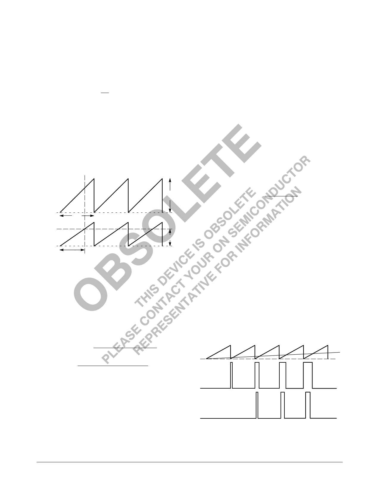
Maximum Duty Cycle
A dedicated internal comparator limits the maximum ON
time of OUT1 by comparing the FF Ramp to VDC(inv). If the
FF Ramp voltage exceeds VDC(inv), the output of the Max
DC Comparator goes high. This will reset the Output Latch,
thus turning OFF the outputs and limiting the duty cycle.
Duty cycle is defined as:
DC
+
ton
T
+
ton
f
Therefore, the maximum ON time can be set to yield the
desired DC if the operating frequency is known. The
maximum ON time is set by adjusting the FF Ramp to reach
VDC(inv) in a time equal to ton(max) as shown in Figure 33.
The maximum ON time should be set for the minimum line
voltage. As line voltage increases, the slope of the FF Ramp
increases. This reduces the duty cycle below DCMAX, which
is a desirable feature as the duty cycle is inversely
proportional to line voltage.
Oscillator Ramp
2V
0V
T
FF Ramp
VDC(inv)
0V
ton(max)
Figure 33. Maximum ON Time Limit Waveforms
An internal resistor divider from a 2.0 V reference is used
to set VDC(inv). If the DCMAX pin is grounded, VDC(inv) is
0.88 V. If the pin is floating, VDC(inv) is 1.19 V. This is
equivalent to 60% or 80% of a 1.5 V FF Ramp. VDC(inv) can
be adjusted to other values by using an external resistor
network on the DCMAX pin. For example, if the minimum
line voltage is 36 V, RFF is 434 kW, operating frequency is
300 kHz and a maximum duty cycle of 70% is required,
VDC(inv) is calculated as follows:
VDC(inv) + IFF
6.7 kW ton(max)
CFF 125 kW
VDC(inv)
+
88.2
mA
10
6.7
pF
kW
125
2.33
kW
ms
+1.10
V
This can be achieved by connecting a 45.3 kW resistor
from the DCMAX pin to GND. The maximum duty cycle
limit can be disabled connecting a 100 kW resistor between
the DCMAX and VREF pins.
5.0 V Reference
The NCP1560 includes a precision 5.0 V reference output.
The reference output is biased directly from VAUX and it can
supply up to 6 mA. Load regulation is 50 mV and line
regulation is 100 mV within the specified operating range.
It is recommended to bypass the reference output with a
0.1 mF ceramic capacitor. The reference output is disabled
when an UV fault is present.
PWM Comparator
The output of an external error amplifier is compared to
the FF Ramp by means of the PWM Comparator. The
external error amplifier drives the VEA input. There is a
0.7 V offset between the VEA input and the PWM
Comparator inverting input. The offset is provided by a
series diode and resistor. If the voltage on the VEA input is
below 0.7 V, the outputs are disabled.
The PWM Comparator controls the duty cycle by turning
OFF the outputs once the FF Ramp voltage exceeds the
offset VEA voltage. The VEA range required to control the
DC from 0% to DCMAX is given by the equation below:
ǒ Ǔ VEA(L) t VEA t
IFF
186.56
DC
pf
f ) VEA(L)
where, VEA(L) is the PWM comparator lower input
threshold.
Soft Start
Soft start (SS) allows the converter to gradually reach
steady state operation, thus reducing start-up stress and
surges on the system. The duty cycle is limited during a soft
start sequence by comparing the Oscillator Ramp to the SS
voltage (VSS) by means of the Soft Start Comparator.
A 6.2 mA current source starts to charge the capacitor on
the SS pin once faults are removed and VAUX reaches 11 V.
The Soft Start Comparator controls the duty cycle while the
SS voltage is below 2.0 V. Once VSS reaches 2.0 V, it exceeds
the Oscillator Ramp voltage and the Soft Start Comparator
does not limit the duty cycle. Figure 34 shows the
relationship between the outputs duty cycle and the soft start
voltage.
Oscillator
Ramp
VSS
OUT2
OUT1
Figure 34. Soft Start Timing Diagram
http://onsemi.com
16
Share Link: 