NCP1560(2003) 데이터 시트보기 (PDF) - ON Semiconductor
부품명
상세내역
일치하는 목록
NCP1560 Datasheet PDF : 18 Pages
| |||
NCP1560
Current Limit
The NCP1560 has two over current protection modes,
cycle by cycle and cycle skip. It allows the NCP1560 to
handle momentary and hard shorts differently for the best
tradeoff in performance and safety. The outputs are disabled
typically 90 ns after a current limit fault is detected.
The cycle by cycle mode terminates the conduction cycle
(reducing the duty cycle) if the voltage on the CS pin
exceeds 0.48 V. The cycle skip mode is enabled if the voltage
on the CS pin reaches 0.57 V. Once a cycle skip fault is
detected, the outputs are disabled, the soft start and cycle
skip capacitors are discharged, and the cycle skip period
(TCSKIP) commences.
VAUX(on)
VAUX
VAUX(off)
0V
NORMAL
ILIM1 ILIM2
OPERATION
RESET
The cycle skip period is set by an external capacitor
(CCSKIP). Once a cycle skip fault is detected, the cycle skip
capacitor is discharged followed by a charge cycle. The
charge current is 12.3 mA. The cycle skip period ends when
the voltage on the cycle skip capacitor reaches 2.0 V. The
cycle skip capacitor is calculated using the equation below:
CCSKIP
[
TCSKIP
2
12.3
V
mA
Using the above equation, a cycle skip period of 11.0 ms
requires a cycle skip capacitor of 68 pF. The differences
between the cycle by cycle and cycle skip modes are
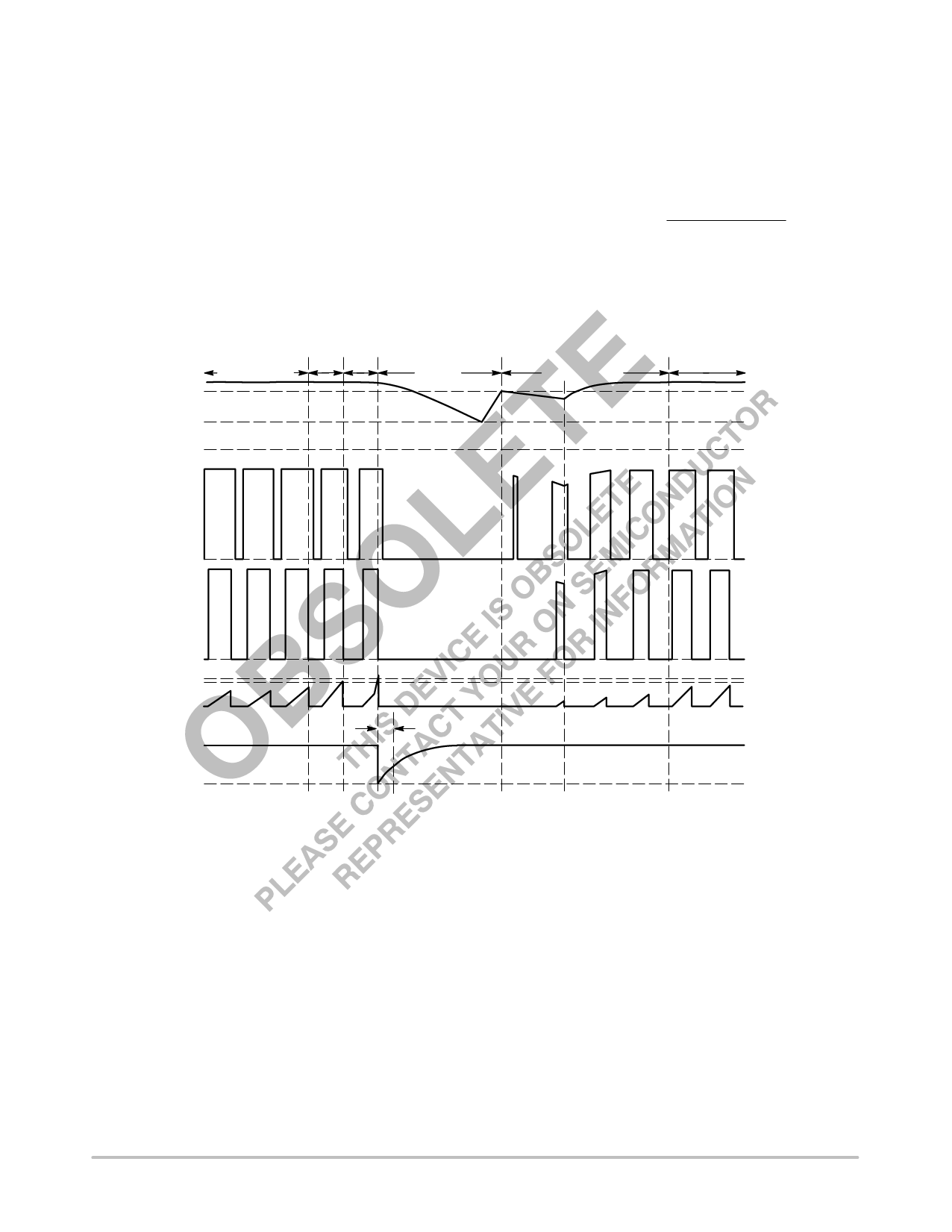
observed in Figure 32.
SOFT START
NORMAL
OPERATION
OUT2
0V
OUT1
0V
ILIM2
ILIM1
CS Voltage
0V
0V
Cycle Skip
Voltage
TCSKIP
Figure 32. Over Current Faults Timing Diagram
Once the cycle skip period is complete and VAUX reaches
11 V, a soft start sequence commences. The possible
minimum OFF time is set by CCSKIP. However, the actual
OFF time is generally greater than the cycle skip period
because it is the cycle skip period added to the time it takes
VAUX to reach 11 V.
Oscillator
The NCP1560 oscillator frequency is set by a single
external resistor connected between the RT pin and GND.
The oscillator is designed to operate up to 500 kHz.
The voltage on the RT pin is laser trim adjusted during
manufacturing to 1.3 V for an RT of 101 kW. A current set
by RT generates an Oscillator Ramp by charging an internal
10 pF capacitor as shown in Figure 2. The period ends
(capacitor is discharged) once the Oscillator Ramp reaches
2.0 V. If RT increases, the current and the Oscillator Ramp
slope decrease, thus reducing the frequency. If RT decreases,
the opposite effect is obtained. Figure 16 shows the
relationship between RT and the oscillator frequency.
http://onsemi.com
15
Share Link: 