LT1613CS5 데이터 시트보기 (PDF) - Linear Technology
부품명
상세내역
일치하는 목록
LT1613CS5 Datasheet PDF : 12 Pages
| |||
U
OPERATIO
effect on loop stability, as long as minimum capacitance
requirements are met). The transient response to a load
step of 50mA to 100mA is pictured in Figure 6. Note the
“double trace,” due to the ESR of C2. The loop is stable and
settles in less than 100µs. In Figure 7, C2 is replaced by a
10µF ceramic unit. Phase margin decreases drastically,
L1
10µH
D1
VIN
2.5V
+ C1
15µF
VIN
SW
LT1613
SHDN
SHDN
FB
GND
R1
37.4k
R2
12.1k
VOUT
5V
+ C2
22µF
C1: AVX TAJA156M010R
C2: AVX TAJA226M006R
D1: MOTOROLA MBR0520
L1: MURATA LQH3C100
1613 F05
Figure 5. 2.5V to 5V Boost Converter with “A”
Case Size Tantalum Input and Output Capacitors
VOUT
20mV/DIV
AC COUPLED
LOAD CURRENT 100mA
50mA
200µs/DIV
1613 F06
Figure 6. 2.5V to 5V Boost Converter Transient
Response with 22µF Tantalum Output Capacitor.
Apparent Double Trace on VOUT Is Due to Switching
Frequency Ripple Current Across Capacitor ESR
LT1613
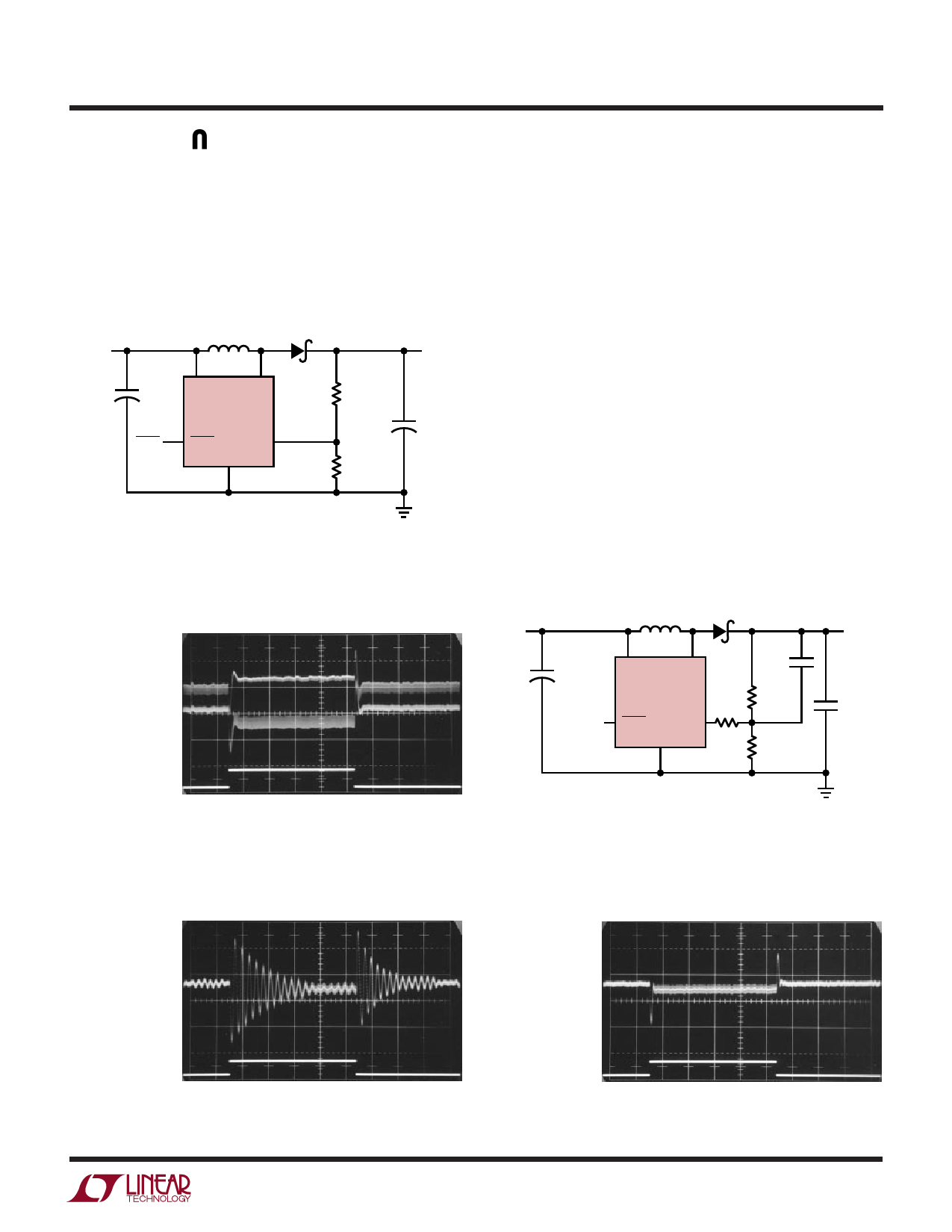
resulting in a severely underdamped response. By adding
R3 and CPL as detailed in Figure 8’s schematic, phase
margin is restored, and transient response to the same
load step is pictured in Figure 9. R3 isolates the device FB
pin from fast edges on the VOUT node due to parasitic PC
trace inductance.
Figure 10’s circuit details a 5V to 12V boost converter,
delivering up to 130mA. The transient response to a load
step of 10mA to 130mA, without CPL, is pictured in
Figure␣ 11. Although the ringing is less than that of the
previous example, the response is still underdamped and
can be improved. After adding R3 and CPL, the improved
transient response is detailed in Figure 12.
Figure 13 shows a SEPIC design, converting a 3V to 10V
input to a 5V output. The transient response to a load step
of 20mA to 120mA, without CPL and R3, is pictured in
Figure␣ 14. After adding these two components, the im-
proved response is shown in Figure 15.
VIN
2.5V
+
C1
15µF
SHUTDOWN
L1
10µH
D1
VIN
SW
LT1613
R3
10k
SHDN
FB
GND
CPL
330pF
R1
37.4k
R2
12.1k
VOUT
5V
C2
10µF
C1: AVX TAJA156M010R
C2: TAIYO YUDEN LMK325BJ106MN
D1: MBR0520
L1: MURATA LQH3C100K04
1613 F08
Figure 8. 2.5V to 5V Boost Converter with Ceramic
Output Capacitor. CPL Added to Increase Phase Margin,
R3 Isolates FB Pin from Fast Edges
VOUT
20mV/DIV
AC COUPLED
VOUT
20mV/DIV
AC COUPLED
LOAD CURRENT
100mA
50mA
200µs/DIV
Figure 7. 2.5V to 5V Boost Converter with
10µF Ceramic Output Capacitor, No CPL
1613 F07
LOAD CURRENT
100mA
50mA
200µs/DIV
1613 F09
Figure 9. 2.5V to 5V Boost Converter with 10µF Ceramic
Output Capacitor, 330pF CPL and 10k in Series with FB Pin
7
Share Link: 