LT1613CS5 데이터 시트보기 (PDF) - Linear Technology
부품명
상세내역
일치하는 목록
LT1613CS5 Datasheet PDF : 12 Pages
| |||
LT1613
PIN FUNCTIONS
SW (Pin 1): Switch Pin. Connect inductor/diode here.
Minimize trace area at this pin to keep EMI down.
GND (Pin 2): Ground. Tie directly to local ground plane.
FB (Pin 3): Feedback Pin. Reference voltage is 1.23V.
Connect resistive divider tap here. Minimize trace area at
FB. Set VOUT according to VOUT = 1.23V(1 + R1/R2).
SHDN (Pin 4): Shutdown Pin. Tie to 1V or more to enable
device. Ground to shut down.
VIN (Pin 5): Input Supply Pin. Must be locally bypassed.
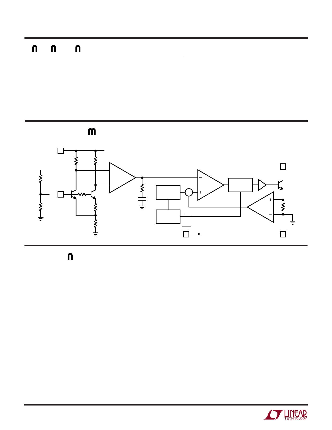
BLOCK DIAGRAM
VIN 5
R5
40k
VOUT
R1
(EXTERNAL)
FB
Q1
FB 3
R2
(EXTERNAL)
VIN
R6
40k
+
A1
gm
–
Q2
x10
R3
30k
R4
140k
U
OPERATIO
– COMPARATOR
A2
RC
RAMP
GENERATOR
Σ
+
CC
FF
R
Q
S
1.4MHz
OSCILLATOR
SHDN
4
SHUTDOWN
1 SW
DRIVER
Q3
0.15Ω
2 GND
1613 • BD
The LT1613 is a current mode, internally compensated,
fixed frequency step-up switching regulator. Operation
can be best understood by referring to the Block Diagram.
Q1 and Q2 form a bandgap reference core whose loop is
closed around the output of the regulator. The voltage
drop across R5 and R6 is low enough such that Q1 and Q2
do not saturate, even when VIN is 1V. When there is no
load, FB rises slightly above 1.23V, causing VC (the error
amplifier’s output) to decrease. Comparator A2’s output
stays high, keeping switch Q3 in the off state. As increased
output loading causes the FB voltage to decrease, A1’s
output increases. Switch current is regulated directly on a
cycle-by-cycle basis by the VC node. The flip flop is set at
the beginning of each switch cycle, turning on the switch.
When the summation of a signal representing switch
current and a ramp generator (introduced to avoid
subharmonic oscillations at duty factors greater than
50%) exceeds the VC signal, comparator A2 changes
state, resetting the flip flop and turning off the switch.
More power is delivered to the output as switch current is
increased. The output voltage, attenuated by external
resistor divider R1 and R2, appears at the FB pin, closing
the overall loop. Frequency compensation is provided
internally by RC and CC. Transient response can be opti-
mized by the addition of a phase lead capacitor CPL in
parallel with R1 in applications where large value or low
ESR output capacitors are used.
As the load current is decreased, the switch turns on for a
shorter period each cycle. If the load current is further
decreased, the converter will skip cycles to maintain
output voltage regulation.
4
Share Link: 