VP2612CGGPFR 데이터 시트보기 (PDF) - Mitel Networks
부품명
상세내역
일치하는 목록
VP2612CGGPFR Datasheet PDF : 11 Pages
| |||
VP2612
values. With a 2Mbits/sec line the error will increase at a rate
of 0.25 bytes per microsecond. Reading the most significant
bytes will trigger the internal latching of the least significant
bytes.
FEC / VMUX Control
This register controls the
operation of the transmission buffer and the FEC block.
Actions taken when bits are set are given below;
BIT
FUNCTION
0
Select 512K buffer. The buffer size must
not be changed during normal operation and must
be defined within 2.4 ms of reset.
1
Enable FEC framing.The option to disable FEC
framing is only provided as a test mode.
2
Force FEC stuffing. If force FEC stuffing is selected
it will start at the beginning of the next frame and
only stop at the start of subsequent frames. The
system processor must ensure that the
transmission buffer does not overflow with forced
stuffing. In normal operation FEC stuffing only
occurs when there is insufficient data in the
transmission buffer.
Bits Per Picture Register When the number of bits which
have been coded has been subtracted from the maximum
possible ( as defined by H.261 ), and the result reaches the
value in this register, then the TOO MANY interrupt will be
generated. The programmed value thus defines in Kbits the
number of bits which may still be generated before reaching
the maximum allowed. The default value is 8 Kbits, and the
maximum number used internally changes between CIF and
QCIF.
INTERRUPT OUTPUTS
The special signals listed below are provided to drive
timers and interrupt inputs on the system processor.
OVERFLOW
FEC STUFF
MACROBLOCK TICK
TOO MANY
( OVR )
( STUFF )
( MTICK )
( TOOM )
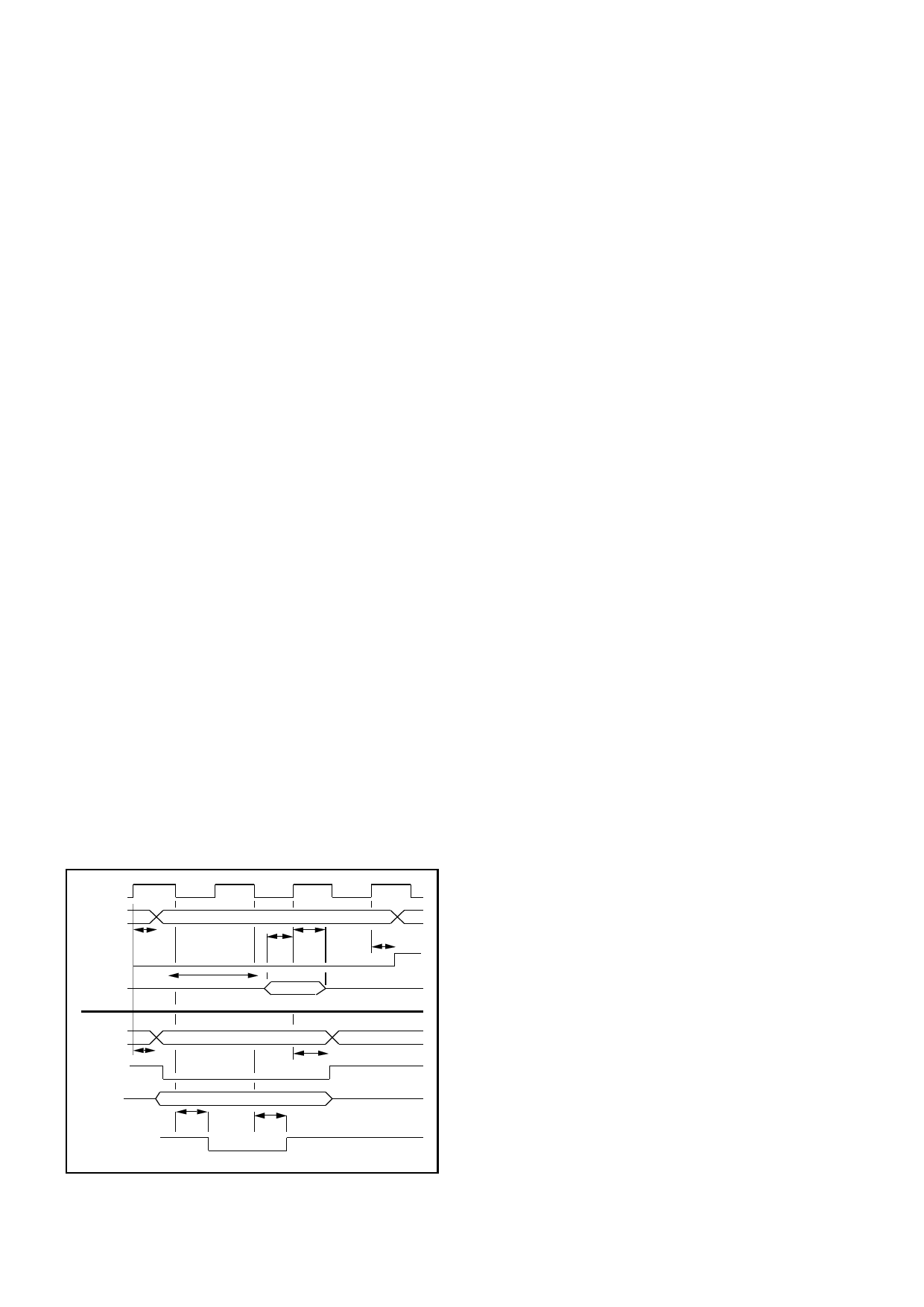
SCLK
ADDRESS
O/P
CHIP ENABLE/
O/P ENEBALE
20ns
max
DATA I/P
ADDRESS
O/P
CHIP
ENABLE
20ns max
DATA
O/P
WRITE
ENABLE
ADDRESS VALID
0ns
15ns min
min
Tac
VALID
WORST CASE READ CYCLE
WRITE CYCLE
20ns
max
20ns
max
DATA VALID
20ns
max
20ns
max
They perform the following functions:
OVR This line signals an impending buffer overflow. When
the buffer reaches 512±128 bits from being full this line will be
taken high, and will remain high until the buffer level falls below
the threshold. It is intended that this line be used as a
processor interrupt, to signal that drastic action must be taken.
STUFF This line signals that FEC stuffing is occuring, and can
be used to monitor the amount of stuffing being performed. It
will pulse high once at the start of each FEC stuffed frame, the
length of the pulse being one line clock period. It is intended
that this should be used to clock a system processor counter,
to keep a running total of the number of FEC stuffed frames.
MTICK This output pulses high once for every Macroblock
received from the VP2611. The pulse is 3 clock cycles in
duration, and the leading edge will occur 6 SCLK cycles after
the Macroblock address was received from the VP2611. It is
anticipated that this should be used to clock a counter in the
system processor, so that the system processor can keep
track of which MB is being processed. In conjunction with the
frame pulse this will enable the system processor to write
information to the VP2611 at appropriate times.
TOOM This signal indicates that the present picture has
reached a threshold relative to the maximum number of bits
per picture allowed by H.261 (256k if CIF, 64k if QCIF). It is set
when the number of bits remaining before the maximum will be
exceeded reaches the value in the Bits Per Picture Register,
and stays high until the end of the current picture.
TRANSMISSION BUFFER INTERFACE
The transmission buffer can consist of either one or
two 32K x 8 bit static RAMs. Fifteen address outputs are
provided for direct connection to the memory devices, and two
RAM select pins are provided to define the device in use. If
only a single device is being used then CE2 is redundant.
An internal FIFO is provided to average out high speed bursts
of transmission buffer cycles. This allows the external SRAM
read cycles to occupy at least three SCLK periods. Detailed
timing for the buffer is given in Figure 5, and shows that with
a 27 MHz clock the RAM must have an access time of less than
39 nanoseconds. Figure 5 illustrates the worst case read
access time, which occurs when a second read cycle follows
the first without an intermediate write cycle. Chip enable and
output enable remain low from the first read cycle.
The write cycle uses two SCLK periods and requires the use
of both the falling and rising edges of SCLK. The Write Enable
output thus remains active for one SCLK period minus
differential rising and falling edge delays. These are limited to
two nanoseconds. Note that when consecutive read or write
operations take place then Chip Enable will remain active, and
not go inactive between cycles.
LINE INTERFACE
A serial interface is provided which facilitates the
operation of the encoder and decoder in a back to back
configuration. It is similar in operation to an X21 interface but
does not support balanced lines. Alternatively the interface
can be used in a simple serial manner by tying the control lines
to fixed logic levels. It uses the following signals:
Figure 5. Transmission Buffer Timing
6
Share Link: 