72605L20 데이터 시트보기 (PDF) - Integrated Device Technology
부품명
상세내역
일치하는 목록
72605L20 Datasheet PDF : 20 Pages
| |||
IDT72605/IDT72615 CMOS SyncBiFIFO
256 x 18 x 2 and 512 x 18 x 2
COMMERCIAL TEMPERATURE RANGE
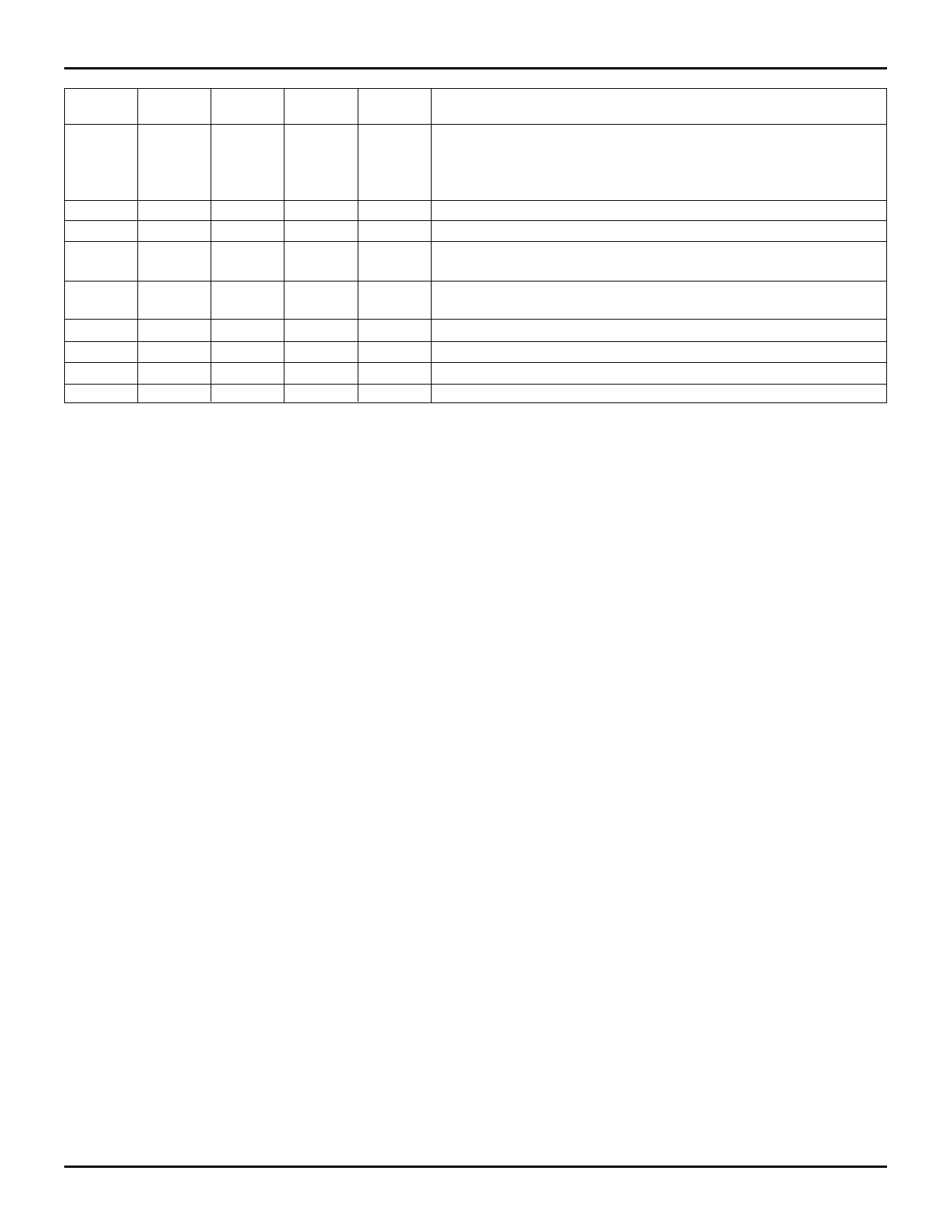
Data A
CSA
R/WA ENA
OEA
I/O
Port A Operation
0
0
0
0
I
Data A is written on CLKA ≠. This write cycle immediately following
low-impedance cycle is prohibited. Note that even though OEA = 0, a
LOW logic level on R/WA, once qualified by a rising edge on CLKA, will
put Data A into a high-impedance state.
0
0
0
1
I
Data A is written on CLKA ≠
0
0
1
X
I
Data A is ignored
0
1
0
0
O
Data is read(1) from RAM array to output register on CLKA ≠,
Data A is low-impedance
0
1
0
1
O
Data is read(1) from RAM array to output register on CLKA ≠,
Data A is high-impedance
0
1
1
0
O
Output register does not change(2), Data A is low-impedance
0
1
1
1
O
Output register does not change(2), Data A is high-impedance
1
0
X
X
I
Data A is ignored(3)
1
1
X
X
O
Data A is high-impedance(3)
NOTES:
2704 tbl 09
1. When A2A1A0 = 000, the next B→A FIFO value is read out of the output register and the read pointer advances. If A2A1A0 = 001, the bypass path is
selected and bypass data from the Port B input register is read from the Port A output register. If A2A1A00 = 1XX, a flag offset register is selected
and its offset is read out through Port A output register.
2. Regardless of the condition of A2A1A0, the data in the Port A output register does not change and the B→A read pointer does not advance.
3. If CSA# is HIGH, then BYPB is HIGH. No bypass occur under this condition.
Table 1. Port A Operation Control Signals
BYPASS PATH
The bypass paths provide direct communication between
Port A and Port B. There are two full 18-bit bypass paths, one
in each direction. During a bypass operation, data is passed
directly between the input and output registers, and the FIFO
memory is undisturbed.
Port A initiates and terminates all bypass operations. The
bypass flag, BYPB, is asserted to inform Port B that a bypass
operation is beginning. The bypass flag state is controlled by
the Port A controls, although the BYPB signal is synchronized
to CLKB. So, BYPB is asserted on the next rising edge of CLKB
when A2A1A0=001and CSA is LOW. When Port A returns to
normal FIFO mode (A2A1A0=000 or CSA is HIGH), BYPB is
deasserted on the next CLKB rising edge.
Once the SyncBiFIFO is in bypass mode, all data transfers
are controlled by the standard Port A (R/WA, CLKA, ENA, OEA)
and Port B (R/WB, CLKB, ENB, OEB) interface pins. Each
bypass path can be considered as a one word deep FIFO.
Data is held in each input register until it is read. Since the
controls of each port operate independently, Port A can be
reading bypass data at the same time Port B is reading bypass
data.
When R/WA and ENA is LOW, data on pins DA0-DA17 is
written into Port A input register. Following the rising edge of
CLKA for this write, the A→B Full Flag (FFAB) goes LOW.
Subsequent writes into Port A are blocked by internal logic
until FFAB goes HIGH again. On the next CLKB rising edge,
the A→B Empty Flag (EFAB) goes HIGH indicating to Port B
that data is available. Once R/WB is HIGH and ENB is LOW,
data is read into the Port B output register. OEB still controls
whether Port B is in a high-impedance state. When OEB is LOW,
the output register data appears at DB0-DB17. EFAB goes LOW
following the CLKB rising edge for this read. FFAB goes HIGH
on the next CLKA rising edge, letting Port A know that another
word can be written through the bypass path.
Bypass data transfers from Port B to Port A work in a similar
manner with EFBA and FFBA indicating the Port A output
register state.
When the Port A address changes from bypass mode
(A2A1A0=001) to FIFO mode (A2A1A0=000) on the rising edge
of CLKA, the data held in the Port B output register may be
overwritten. Unless Port A monitors the BYPB pin and waits
for Port B to clock out the last bypass word, data from the A→B
FIFO will overwrite data in the Port B output register. BYPB will
go HIGH on the rising edge of CLKB signifying that Port B has
finished its last bypass operation. Port B must read any
bypass data in the output register on this last CLKB clock or it
is lost and the SyncBiFIFO returns to FIFO operations. It is
especially important to monitor BYPB when CLKB is much
slower than CLKA to avoid this condition. BYPB will also go
HIGH after CSA is brought HIGH; in this manner the Port B
bypass data may also be lost.
Since the Port A processor controls CSA and the bypass
mode, this scenario can be handled for B→A bypass data. The
Port A processor must be set up to read the last bypass word
before leaving bypass mode.
5.18
8
Share Link: 