IDT72605(2013) 데이터 시트보기 (PDF) - Integrated Device Technology
부품명
상세내역
일치하는 목록
IDT72605 Datasheet PDF : 17 Pages
| |||
IDT72605/72615 CMOS SYNCBiFIFO™
256 x 18x 2 and 512 x 18 x 2
can be written or read in Port B. If R/WB and ENB are LOW, data is written into
input register, and on LOW-to-HIGH transition of CLKB data is written into input
register and the FIFO memory. If R/WB is HIGH and OEB is LOW, data comes
out of bus and is read from output register into three-state buffer. In bypass mode,
INDUSTRIAL TEMPERATURE RANGE
if R/WB is LOW, bypass messages are transferred into B→A output register.
If R/WA is HIGH, bypass messages are transferred into A→B output register.
Refer to pin descriptions for more information.
TABLE 3 ⎯ FLAG OFFSET REGISTER FORMAT
PAEAB Register
17 16 15 14 13 12 11 10 9 8 7 6 5 4 3 2 1 0
XXXXXXXXX
A→B FIFO Almost-Empty Flag Offset
PAFAB Register
17 16 15 14 13 12 11 10 9 8 7 6 5 4 3 2 1 0
XXXXXXXXX
A→B FIFO Almost-Full Flag Offset
PAEBA Register
17 16 15 14 13 12 11 10 9 8 7 6 5 4 3 2 1 0
XXXXXXXXX
B→A FIFO Almost-Empty Flag Offset
PAFBA Register
17 16 15 14 13 12 11 10 9 8 7 6 5 4 3 2 1 0
XXXXXXXXX
B→A FIFO Almost-Full Flag Offset
NOTE:
1. Bit 8 must be set to 0 for the IDT72605 (256 x 18) Synchronous BiFIFO.
TABLE 4 ⎯ INTERNAL FLAG TRUTH TABLE
Number of Words
in FIFO
From
To
EF
0
0
LOW
1
n
HIGH
n+1
D-(m+1)
HIGH
D-m
D-1
HIGH
D
D
HIGH
NOTE:
1. n = Programmable Empty Offset (PAEAB Register or PAEBA Register)
m = Programmable Full Offset (PAFAB Register or PAFBA Register)
D = FIFO Depth (IDT72605 = 256 words, IDT72615= 512 words)
PAE
LOW
LOW
HIGH
HIGH
HIGH
PAF
HIGH
HIGH
HIGH
LOW
LOW
FF
HIGH
HIGH
HIGH
HIGH
LOW
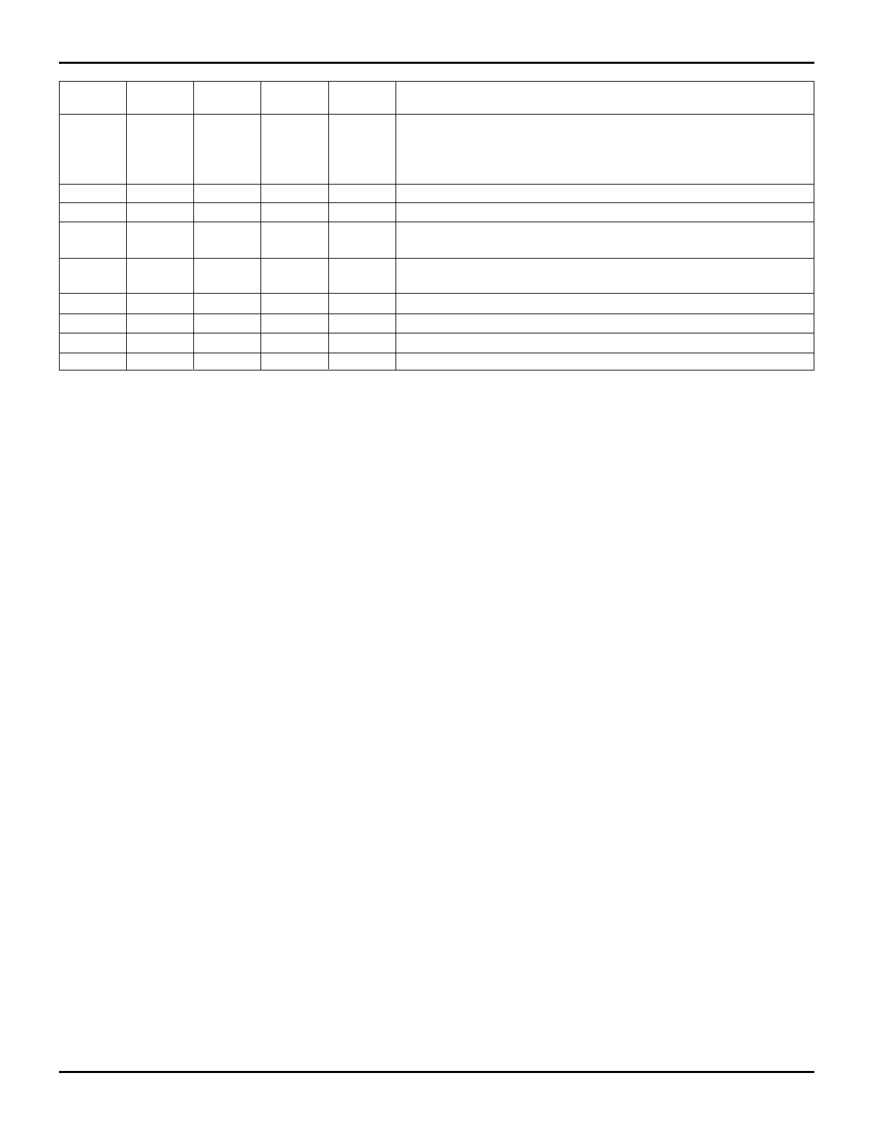
TABLE 5 ⎯ PORT B OPERATION CONTROL SIGNALS
R/WB
ENB
Data B
OEB
I/O
Port B Operation
0
0
0
I
Data B is written on CLKB ↑. This write cycle immediately following output low-impedance cycle is prohibited. Note
that even though OEB = 0, a LOW logic level on R/WB, once qualified by a rising edge on CLKB, will put Data B into a high-
impedance state.
0
0
1
I
Data B is written on CLKB ↑.
0
1
X
I
Data B is ignored
1
0
0
O
Data is read(1) from RAM array to output register on CLKB ≠ Data B is low-impedance
1
0
1
O
Data is read(1) from RAM array to output register on CLKB ≠, Data B is high- impedance
1
1
0
O
Output register does not change(2), Data B is low-impedance
1
1
1
O
Output register does not change(2), Data B is high-impedance
NOTES:
1. When A2A1A0 = 000 or 1XX, the next A→B FIFO value is read out of the output register and the read pointer advances. If A2A1A0 = 001, the bypass path is selected and
bypass data is read from the Port B output register.
2. Regardless of the condition of A2A1A0, the data in the Port B output register does not change and the A→B read pointer does not advance.
8
Share Link: 