CDP1879 데이터 시트보기 (PDF) - Intersil
부품명
상세내역
일치하는 목록
CDP1879 Datasheet PDF : 18 Pages
| |||
CDP1879, CDP1879C-1
FREEZE
CIRCUIT
AM - PM
AND
HOUR LOGIC
CALENDAR
LOGIC
XTAL
OSCILLATOR
XTAL
PRESCALE
SECOND
MINUTE
HOUR
DAY
MONTH
PRESCALE CLOCK
SELECT SELECT
CLOCK OUT
INT
RESET
VDD
CLOCK AND
INT. LOGIC
VSS
CONTROL
REGISTER
INT. STATUS
REGISTER
8-BIT DATA BUS
COMPARATOR
SECOND
LATCH
MINUTE
LATCH
HOUR
LATCH
I/O
INTERFACE
DB0-DB7
A0
A1
A2
TPA
IO/MEM
TPB/WR
RD
CS
POWER DOWN
ADDRESS DECODE
AND
CONTROL LOGIC
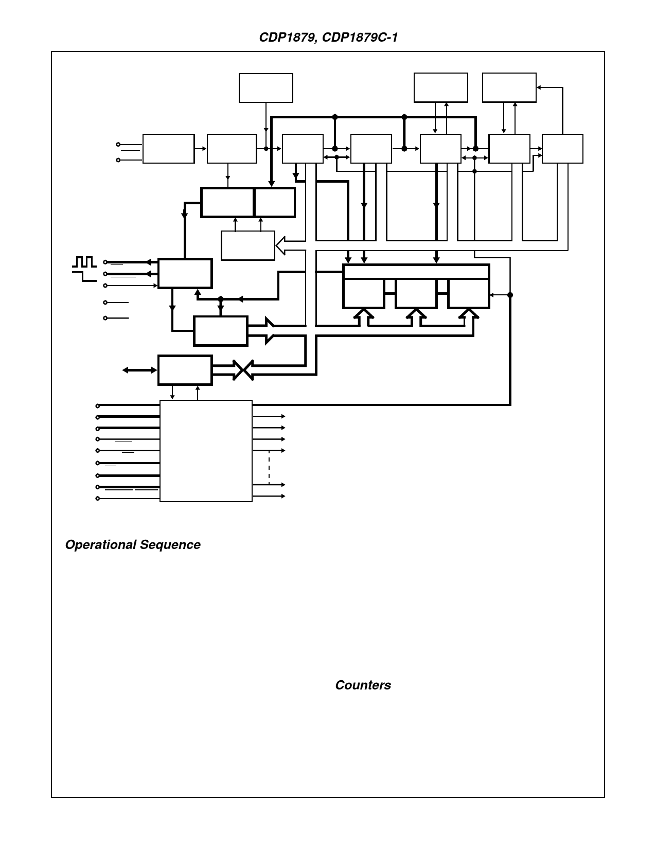
FIGURE 3. FUNCTIONAL DIAGRAM - ALARM CIRCUIT, CLOCK OUTPUT, INTERRUPT, AND STATUS REGISTERS HIGHLIGHTED
Operational Sequence
Power is applied and the real-time clock is reset. This sets
the interrupt output pin high. After the CS pin is set high and
with address 7 on the address input lines, the control register
is loaded via the data bus to configure the clock.
With selective addressing, the seconds through month
counters are then written to and loaded to set the current time.
The real-time clock will now hold the current “wall clock” time,
with an accuracy determined by the crystal or external clock
used. If the alarm function is desired, the control register is
accessed and loaded again. This new byte will allow subse-
quent time data to be entered into the seconds, minutes and
hours alarm latches. This sequence is also used when select-
ing one of the 15 available clock-out signals.
If the alarm function was selected, the interrupt output pin
will be set low when the values in the seconds, minutes and
hour alarm latches match those in the seconds, minutes and
hour counters.
If one of the 15 sub second-to-day clock outputs is selected
by the byte in the control register, the clock output pin tog-
gles at that frequency (50% duty cycle) The interrupt output
will also be set low on the first clock out negative transition.
The interrupt source (alarm or clock out) can be determined
by reading the interrupt status register. The clock output can
be deselected by placing zero in the upper nibble of the con-
trol register if the alarm function is selected as the only inter-
rupt source.
Counters
The counter section consists of an on-board oscillator, a
prescaler and 5 counters that hold the time of day/calendar
information (see Figure 2).
1 of 4 possible external crystals determine the frequency of the
on-board oscillator (32,768Hz, 1.048576MHz, 2.097152MHz,
4.194304MHz). The oscillator output is divided down by a pres-
4-111
Share Link: 