TLE4254 데이터 시트보기 (PDF) - Infineon Technologies
부품명
상세내역
일치하는 목록
TLE4254 Datasheet PDF : 21 Pages
| |||
TLE4254
Electrical Characteristics
5
Electrical Characteristics
5.1
Tracking Regulator
The output voltage VQ is controlled by comparing it to the voltage applied at pin ADJ/EN and driving a PNP pass
transistor accordingly. The control loop stability depends on the output capacitor CQ, the load current, the chip
temperature and the poles/zeros introduced by the integrated circuit and the load. To ensure stable operation, the
output capacitor’s capacitance and its equivalent series resistor ESR requirements given in the table “Functional
Range” have to be maintained. For details see also the typical performance graph “Output Capacitor Series
Resistor ESRCQ vs. Output Current IQ”. Also, the output capacitor shall be sized to buffer load transients.
An input capacitor CI is strongly recommended to buffer line influences. Connect the capacitors close to the IC
terminals.
Protection circuitry prevent the IC as well as the application from destruction in case of catastrophic events. These
safeguards contain output current limitation, reverse polarity protection as well as thermal shutdown in case of
overtemperature.
In order to avoid excessive power dissipation that could never be handled by the pass element and the package,
the maximum output current is decreased at high input voltages.
The overtemperature protection circuit prevents the IC from immediate destruction under fault conditions (e. g.
output continuously short-circuited) by reducing the output current. A thermal balance below 200 °C junction
temperature is established. Please note that a junction temperature above 150 °C is outside the maximum ratings
and reduces the IC lifetime.
The TLE4254 allows a negative supply voltage. However, several small currents are flowing into the IC increasing
its junction temperature. This has to be considered for the thermal design, respecting that the thermal protection
circuit is not operating during reverse polarity condition.
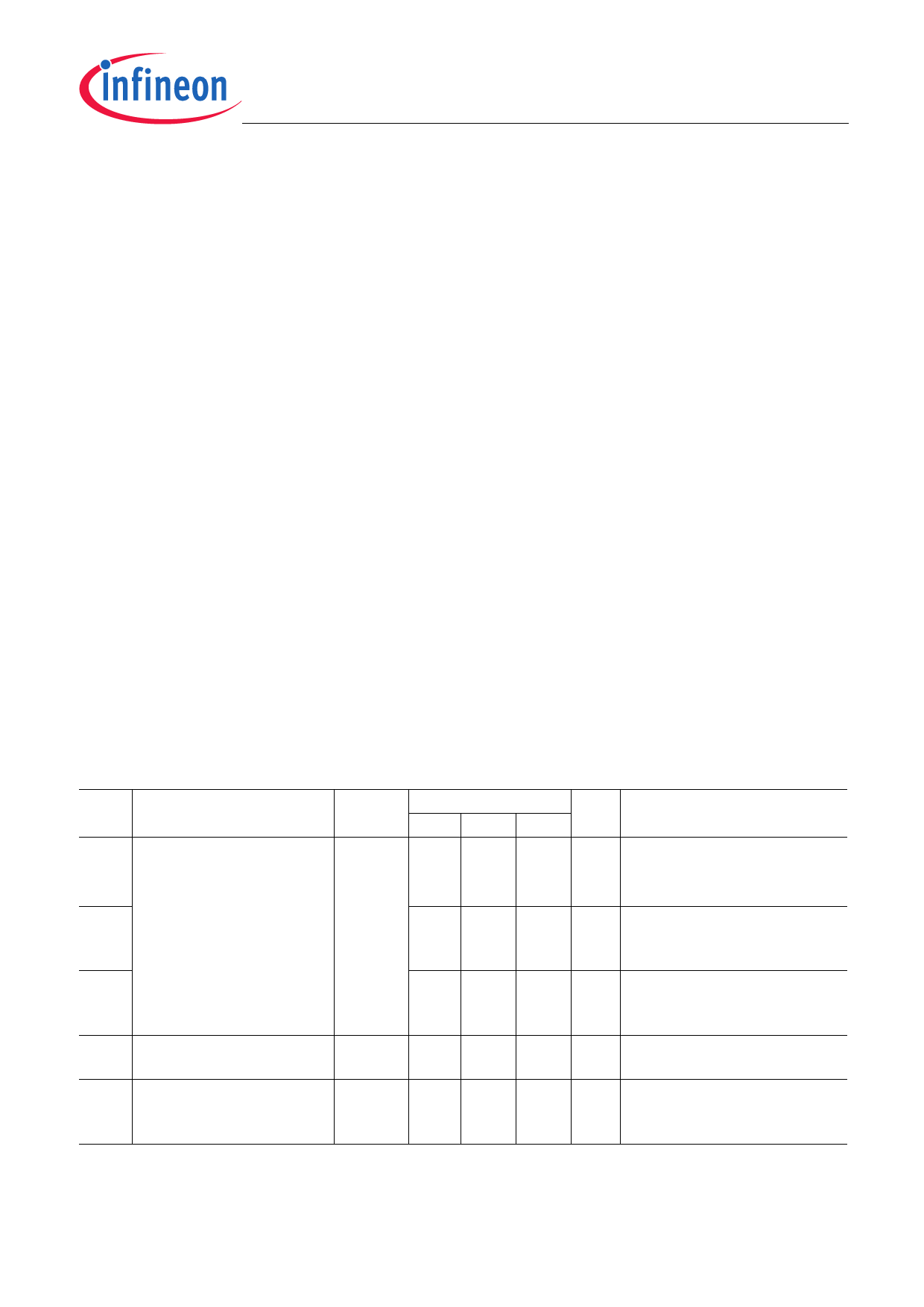
Table 1 Electrical Characteristics Tracking Regulator
VI = 13.5 V; VADJ/EN ≥ 2.0 V; VFB = VQ (version GA / EJ A); -40 °C ≤ Tj ≤ 150 °C; CQ = 1 µF;
all voltages with respect to ground (unless otherwise specified).
Pos. Parameter
Symbol
Limit Values
Unit Test Condition
Min. Typ. Max.
5.1.1 Output Voltage Tracking ∆VQ
Accuracy
∆VQ = VEN/ADJ - VQ
5.1.2
-5 –
-10 –
5.1.3
-10 –
5.1.4
5.1.5
Load Regulation
steady-state
Line Regulation
steady-state
|dVQ,load| –
1
|dVQ,line| –
1
5
mV 8 V ≤ VI ≤ 18 V;
0.1 mA ≤ IQ ≤ 60 mA;
VADJ/EN = 5 V
10
mV 5.5 V ≤ VI ≤ 26 V;
0.1 mA ≤ IQ ≤ 60 mA;
VADJ/EN = 5 V
10
mV 5.5 V ≤ VI ≤ 32 V;
0.1 mA ≤ IQ ≤ 30 mA;
VADJ/EN = 5 V
10
mV IQ = 0.1 mA to 70 mA;
VADJ/EN = 5 V
10
mV VI = 5.5 V to 32 V;
IQ = 5 mA
VADJ/EN = 5 V
Data Sheet
8
Rev. 1.2, 2009-11-18
Share Link: 