TLE4254 데이터 시트보기 (PDF) - Infineon Technologies
부품명
상세내역
일치하는 목록
TLE4254 Datasheet PDF : 21 Pages
| |||
TLE4254
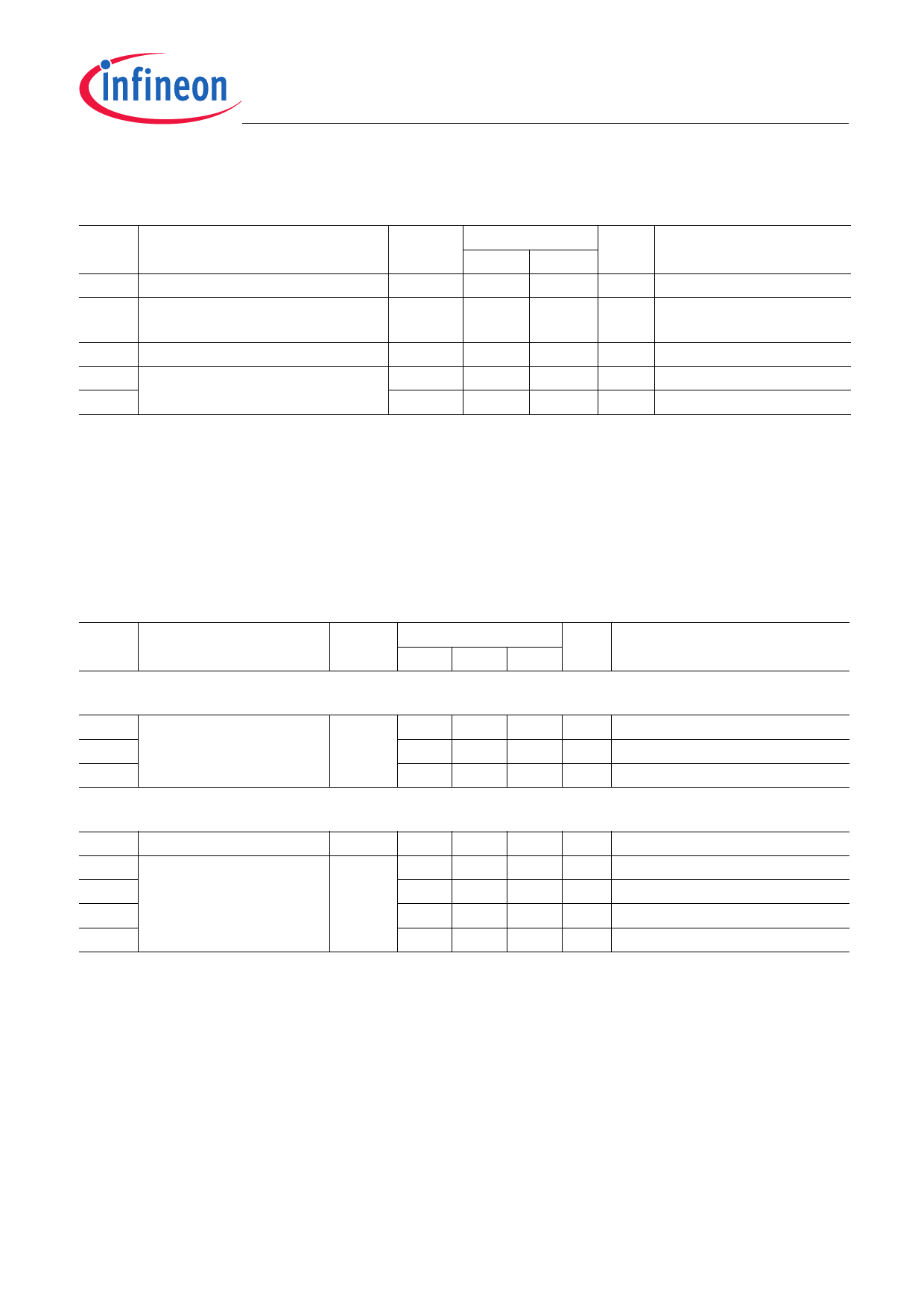
General Product Characteristics
4.2
Functional Range
Pos. Parameter
Symbol
4.2.1
4.2.1
Input Voltage
Adjust / Enable Input Voltage
(Voltage Tracking Range)
VI
VADJ/EN
4.2.2 Junction Temperature
Tj
4.2.3 Output Capacitor
CQ
4.2.4
ESRCQ
1) Not subject to production test; specified by design.
Limit Values
Min. Max.
4
45
2.0
–
-40
150
1
–
–
5
Unit
V
V
°C
µF
Ω
Conditions
VI ≥ VQ + Vdr
–
–
– 1)
– 1)
Note: Within the functional range the IC operates as described in the circuit description. The electrical
characteristics are specified within the conditions given in the related electrical characteristics table.
4.3
Thermal Resistance
Pos. Parameter
Symbol
Limit Values
Unit Conditions
Min. Typ. Max.
PG-DSO-8:
4.3.1 Junction to Ambient
4.3.2
4.3.3
RthJA
–
–
–
155 –
96 –
86 –
K/W
K/W
K/W
Footprint only 1) 2)
300 mm2 PCB heatsink area 1) 2)
600 mm2 PCB heatsink area 2) 1)
PG-DSO-8 exposed pad:
4.3.4
4.3.5
4.3.6
Junction to Case
Junction to Ambient
RthJC
–
RthJA
–
–
15 –
47 –
159 –
K/W
K/W
K/W
measured to exposed pad
–3)
Footprint only 2) 1)
4.3.7
–
71 –
K/W 300 mm2 PCB heatsink area 2) 1)
4.3.8
–
60 –
K/W 600 mm2 PCB heatsink area 2) 1)
1) Not subject to production test; specified by design.
2) Package mounted on PCB FR4; 80 x 80 x 1.5 mm; 35 µm Cu, 5 µm Sn; horizontal position; zero airflow.
3) Specified RthJA value is according to Jedec JESD51-2,-5,-7 at natural convection on FR4 2s2p board; The Product
(Chip+Package) was simulated on a 76.2 x 114.3 x 1.5 mm³ board with 2 inner copper layers (2 x 70µm Cu, 2 x 35µm Cu).
Where applicable a thermal via array under the exposed pad contacted the first inner copper layer.
Data Sheet
7
Rev. 1.2, 2009-11-18
Share Link: 