TLE4254 데이터 시트보기 (PDF) - Infineon Technologies
부품명
상세내역
일치하는 목록
TLE4254 Datasheet PDF : 21 Pages
| |||
3
Pin Definitions and Functions
3.1
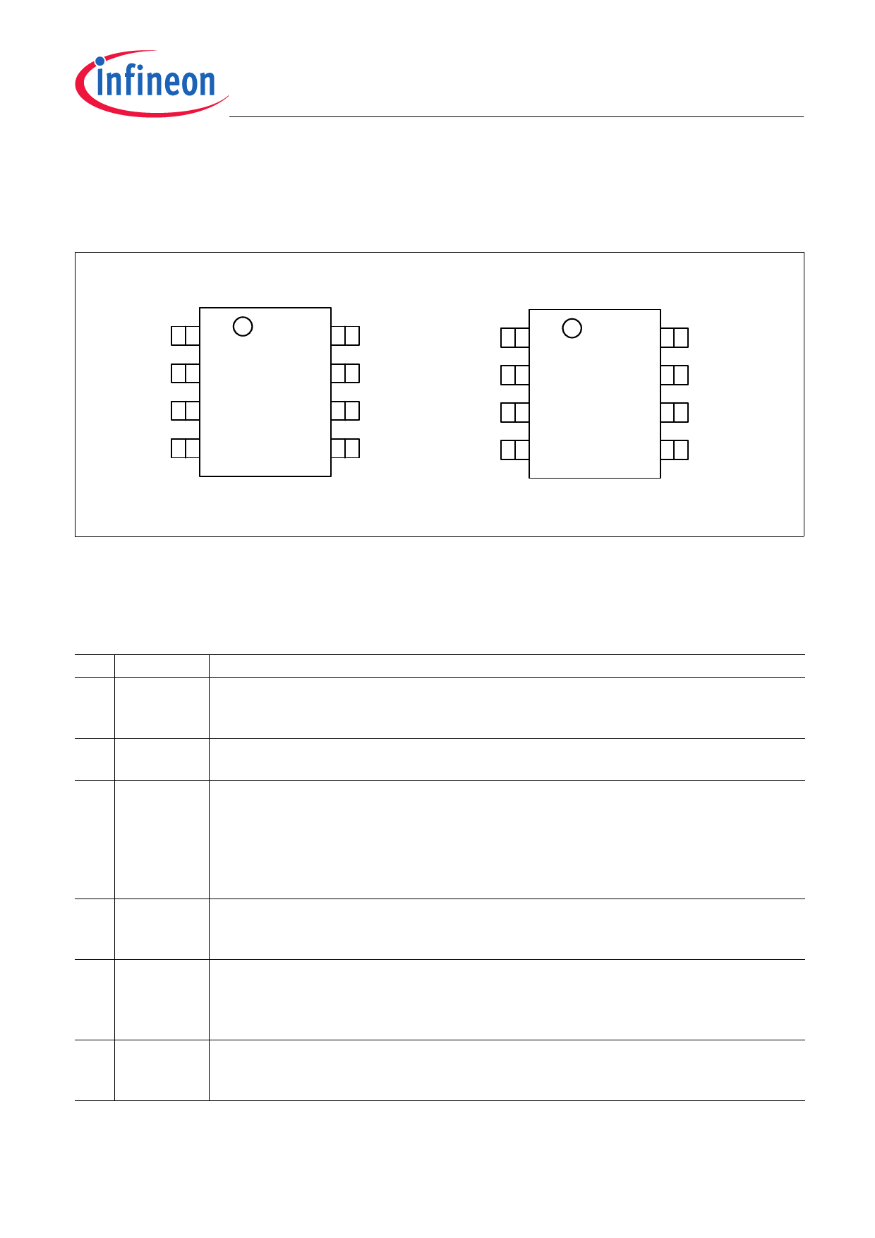
Pin Assignment TLE4254GA and TLE4254GS
TLE4254
Pin Definitions and Functions
Q
GND
GND
FB
1
8
2 TLE 4254 7
3
GA
6
4
5
I
GND
GND
EN/ADJ
Q
GND
GND
ST
1
8
2 TLE 4254 7
GS
3
6
4
5
I
GND
GND
EN/ADJ
Figure 3 Pin Configurations TLE4254GA and TLE4254GS
3.2
Pin Functions TLE4254GA and TLE4254GS
Pin Symbol
Function
1Q
Tracker Output.
Block to GND with a capacitor close to the IC terminals, respecting capacitance and ESR
requirements given in the table “Functional Range”.
2, 3, GND
6, 7
Ground reference.
Interconnect the pins on PCB. Connect to heatsink area.
4 FB
Feedback input (version GA only).
(version GA) Non inverting input of the internal error amplifier to control the output voltage.
Connect this pin directly to the output pin in order to obtain lower or equal output voltages
with respect to the reference voltage.
Connect a voltage divider for higher output voltages than the reference.
(See also application information.)
4 ST
Tracking Regulator Status Output (version GS only).
(version GS) Open collector output. Connect via a pull-up resistor to a positive voltage rail.
A low signal indicates fault condions at the regulator’s output.
5 EN/ADJ
Adjust / Enable.
Connect the reference to this pin. The active high signal of the reference turns on the device;
a low signal disables the IC. The reference voltage can be connected directly or by a voltage
divider for lower output voltages (see application information).
8I
Input.
IC supply. For compensating line influences, a capacitor close to the IC terminals is
recommended.
Data Sheet
4
Rev. 1.2, 2009-11-18
Share Link: 