PCK2010RDL 데이터 시트보기 (PDF) - Philips Electronics
부품명
상세내역
일치하는 목록
PCK2010RDL Datasheet PDF : 18 Pages
| |||
Philips Semiconductors
CK98R (100/133MHz) RCC spread spectrum
system clock generator
Product specification
PCK2010R
FEATURES
• Mixed 2.5 V and 3.3 V operation
• Four CPU clocks at 2.5 V
• Eight PCI clocks at 3.3 V, one free-running
(synchronous with CPU clocks)
• Four 3.3 V fixed clocks @ 66 MHz
• Two 2.5 V CPUDIV2 clocks @ ½ CPU clock frequency
• Three 2.5 V IOAPIC clocks @ 16.67 MHz
• One 3.3 V 48 MHz USB clock
• Two 3.3 V reference clocks @ 14.318 MHz
• Reference 14.31818 MHz Xtal oscillator input
• 133 MHz or 100 MHz operation
• Power management control input pins
• CPU clock jitter ≤ 250 ps cycle-cycle
• CPU clock skew ≤ 175 ps pin-pin
• 0.0ns – 1.5 ns CPU - 3V66 delay
• 1.5ns – 3.5 ns 3V66 - PCI delay
• 1.5ns – 4.0 ns CPU - IOAPIC delay
• 1.5ns – 4.0 ns CPU - PCI delay
• Available in 56-pin SSOP package
• ±0.5% center spread spectrum capability via select pins
• –0.5% down spread spectrum capability via select pins
DESCRIPTION
The PCK2010R is a clock generator (frequency synthesizer) chip for
a Pentium II and other similar processors.
The PCK2010R has four CPU clock outputs at 2.5 V, two CPUDIV2
clock outputs running at ½ CPU clock frequency (66 MHz or 50 MHz
depending on the state of SEL133/100) and four 3V66 clocks
running at 66MHz. There are eight PCI clock outputs running at
33 MHz. One of the PCI clock outputs is free-running. Additionally,
the part has three 2.5 V IOAPIC clock outputs at 16.67 MHz and two
3.3 V reference clock outputs at 14.318 MHz. All clock outputs meet
Intel’s drive strength, rise/fall time, jitter, accuracy, and skew
requirements.
The part possesses dedicated power-down, CPUSTOP, and
PCISTOP input pins for power management control. These inputs
are synchronized on-chip and ensure glitch-free output transitions.
When the CPUSTOP input is asserted, the CPU clock outputs and
3V66 clock outputs are driven LOW. When the PCISTOP input is
asserted, the PCI clock outputs are driven LOW.
Finally, when the PWRDWN input pin is asserted, the internal
reference oscillator and PLLs are shut down, and all outputs are
driven LOW.
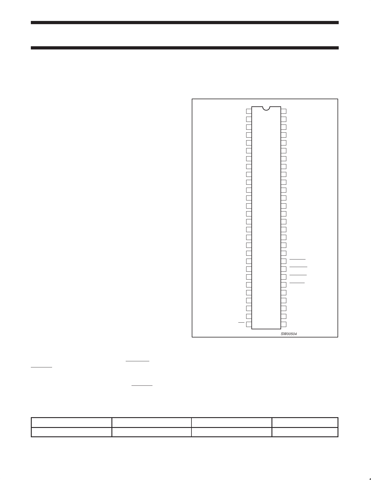
PIN CONFIGURATION
VSS 1
REF0 2
REF1 3
VDD3V 4
XTAL_IN 5
XTAL_OUT 6
VSS 7
PCICLK_F 8
PCICLK1 9
VDD3V 10
PCICLK2 11
PCICLK3 12
VSS 13
PCICLK4 14
PCICLK5 15
VDD3V 16
PCICLK6 17
PCICLK7 18
VSS 19
VSS 20
3V66_0 21
3V66_1 22
VDD3V 23
VSS 24
3V66_0 25
3V66_1 26
VDD3V 27
SEl133/100 28
56 VDD25V
55 APIC2
54 APIC1
53 APIC0
52 VSS
51 VDD25V
50 CPUDIV2_1
49 CPUDIV2_0
48 VSS
47 VDD25V
46 CPUCLK3
45 CPUCLK2
44 VSS
43 VDD25V
42 CPUCLK1
41 CPUCLK0
40 VSS
39 VDD3V
38 VSS
37 PCISTOP
36 CPUSTOP
35 PWRDWN
34 SPREAD
33 SEL1
32 SEL0
31 VDD3V
30 48MHz_USB
29 VSS
SW00504
ORDERING INFORMATION
PACKAGES
TEMPERATURE RANGE
56-Pin plastic SSOP
0°C to +70°C
Intel and Pentium are registered trademarks of Intel Corporation.
ORDER CODE
PCK2010R DL
DRAWING NUMBER
SOT371-1
1999 Oct 19
2
853–2179 22543
Share Link: 