K30A06N1 데이터 시트보기 (PDF) - Toshiba
부품명
상세내역
일치하는 목록
K30A06N1 Datasheet PDF : 9 Pages
| |||
TK30A06N1
6. Electrical Characteristics
6.1. Static Characteristics (Ta = 25 unless otherwise specified)
Characteristics
Symbol
Test Condition
Min Typ. Max Unit
Gate leakage current
IGSS
VGS = ±20 V, VDS = 0 V
±0.1
µA
Drain cut-off current
IDSS
VDS = 60 V, VGS = 0 V
10
Drain-source breakdown voltage
Drain-source breakdown voltage
(Note 4)
V(BR)DSS ID = 10 mA, VGS = 0 V
V(BR)DSX ID = 10 mA, VGS = -20 V
60
V
45
Gate threshold voltage
Vth
VDS = 10 V, ID = 0.2 mA
2.0
4.0
Drain-source on-resistance
RDS(ON) VGS = 10 V, ID = 15 A
12.2 15.0 mΩ
Note 4: If a reverse bias is applied between gate and source, this device enters V(BR)DSX mode. Note that the drain-
source breakdown voltage is lowered in this mode.
6.2. Dynamic Characteristics (Ta = 25 unless otherwise specified)
Characteristics
Input capacitance
Reverse transfer capacitance
Output capacitance
Gate resistance
Switching time (rise time)
Switching time (turn-on time)
Switching time (fall time)
Switching time (turn-off time)
Symbol
Test Condition
Ciss
Crss
Coss
rg
tr
ton
tf
toff
VDS = 30 V, VGS = 0 V, f = 1 MHz
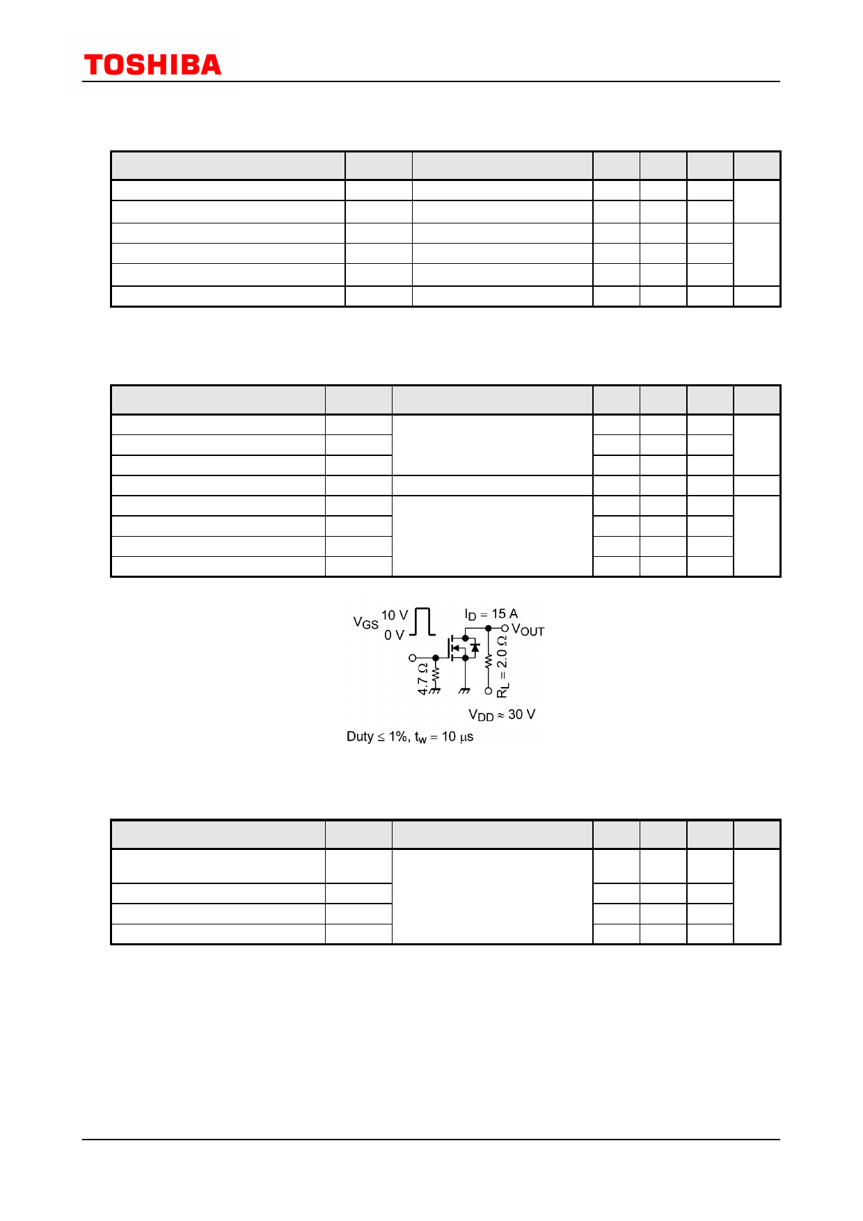
See Figure 6.2.1.
Min Typ. Max Unit
1050
pF
33
400
3.9
Ω
7.3
ns
21
7.3
28
Fig. 6.2.1 Switching Time Test Circuit
6.3. Gate Charge Characteristics (Ta = 25 unless otherwise specified)
Characteristics
Total gate charge (gate-source plus
gate-drain)
Gate-source charge 1
Gate-drain charge
Gate switch charge
Symbol
Test Condition
Qg
VDD ≈ 48 V, VGS = 10 V, ID = 30 A
Qgs1
Qgd
QSW
Min Typ. Max Unit
16
nC
5.2
4.4
6.8
3
2012-09-20
Rev.4.0
Share Link: 