TC58NVG0S3AFT05 데이터 시트보기 (PDF) - Toshiba
부품명
상세내역
일치하는 목록
TC58NVG0S3AFT05 Datasheet PDF : 33 Pages
| |||
TC58NVG0S3AFT05
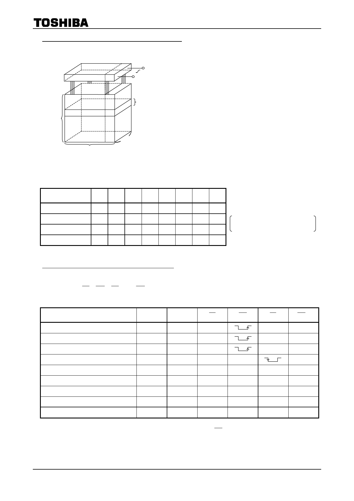
Schematic Cell Layout and Address Assignment
The Program operation works on page units while the Erase operation works on block units.
2048
64
I/O1
I/O8
65536
pages
1024 blocks
64 Pages
= 1 block
8I/O
2112
Figure 2. Schematic Cell Layout
A page consists of 2112 bytes in which 2048 bytes are used
for main memory storage and 64 bytes are for redundancy
or for other uses.
1 page = 2112 bytes
1 block = 2112 bytes × 64 pages = (128K + 4K) bytes
Capacity = 2112 bytes × 64 pages × 1024 blocks
An address is read in via the I/O port over four consecutive
clock cycles, as shown in Table 1.
Table 1. Addressing
First cycle
Second cycle
Third cycle
Fourth cycle
I/O8 I/O7 I/O6 I/O5 I/O4 I/O3 I/O2 I/O1
CA7 CA6 CA5 CA4 CA3 CA2 CA1 CA0
L
L
L
L CA11 CA10 CA9 CA8
PA7 PA6 PA5 PA4 PA3 PA2 PA1 PA0
PA15 PA14 PA13 PA12 PA11 PA10 PA9 PA8
CA0 to CA11: Column address
PA0 to PA15 : Page address
PA6 to PA15 : Block address
PA0 to PA5 : NAND address in block
Operation Mode: Logic and Command Tables
The operation modes such as Program, Erase, Read and Reset are controlled by the eleven different
command operations shown in Table 3. Address input, command input and data input/output are controlled by
the CLE, ALE, CE , WE , RE and WP signals, as shown in Table 2.
Table 2. Logic Table
CLE
ALE
CE
WE
RE
WP *1
Command Input
H
L
L
H
*
Data Input
L
L
L
H
H
Address input
L
H
L
H
*
Serial Data Output
L
L
L
H
*
During Programming (Busy)
*
*
*
*
*
H
During Erasing (Busy)
*
*
*
*
*
H
During Reading (Busy)
*
*
*
*
*
*
Program, Erase Inhibit
*
*
*
*
*
L
Standby
*
*
H
*
*
0 V/VCC
H: VIH, L: VIL, *: VIH or VIL
*1: Refer to Application Note (10) toward the end of this document regarding the WP signal when Program or Erase Inhibit
2003-08-20A 16/33
Share Link: 