TC58NVG0S3AFT05 데이터 시트보기 (PDF) - Toshiba
부품명
상세내역
일치하는 목록
TC58NVG0S3AFT05 Datasheet PDF : 33 Pages
| |||
TC58NVG0S3AFT05
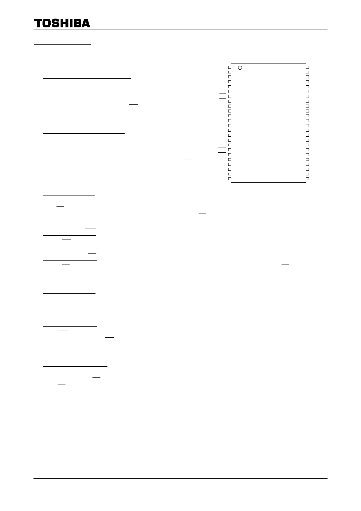
PIN FUNCTIONS
The device is a serial access memory which utilizes time-sharing input of address information. The device
pin-outs are configured as shown in Figure 1.
Command Latch Enable: CLE
The CLE input signal is used to control loading of the
operation mode command into the internal command register.
The command is latched into the command register from the
I/O port on the rising edge of the WE signal while CLE is
High.
Address Latch Enable: ALE
The ALE signal is used to control loading of either address
information or input data into the internal address/data
register.
Address information is latched on the rising edge of WE if
ALE is High.
Input data is latched if ALE is Low.
NC 1
NC 2
NC 3
NC 4
NC 5
GND 6
RY/BY 7
RE 8
CE 9
NC 10
NC 11
VCC 12
VSS 13
NC 14
NC 15
CLE 16
ALE 17
WE 18
WP 19
NC 20
NC 21
NC 22
NC 23
NC 24
48 NC
47 NC
46 NC
45 NC
44 I/O8
43 I/O7
42 I/O6
41 I/O5
40 NC
39 NC
38 NC
37 VCC
36 VSS
35 NC
34 NC
33 NC
32 I/O4
31 I/O3
30 I/O2
29 I/O1
28 NC
27 NC
26 NC
25 NC
Chip Enable: CE
Figure 1. Pinout
The device goes into a low-power Standby mode when CE goes High during the device is in Ready state.
The CE signal is ignored when device is in Busy state ( RY / BY = L), such as during a Program or Erase or
Read operation, and will not enter Standby mode even if the CE input goes High.
Write Enable: WE
The WE signal is used to control the acquisition of data from the I/O port.
Read Enable: RE
The RE signal controls serial data output. Data is available tREA after the falling edge of RE .
The internal column address counter is also incremented (Address = Address + 1) on this falling edge.
I/O Port: I/O1 to 8
The I/O1 to 8 pins are used as a port for transferring address, command and input/output data to and from
the device.
Write Protect: WP
The WP signal is used to protect the device from accidental programming or erasing. The internal voltage
regulator is reset when WP is Low. This signal is usually used for protecting the data during the power-on/off
sequence when input signals are invalid.
Ready/Busy: RY / BY
The RY / BY output signal is used to indicate the operating condition of the device. The RY / BY signal is
in Busy state ( RY / BY = L) during the Program, Erase and Read operations and will return to Ready state
( RY / BY = H) after completion of the operation. The output buffer for this signal is an open drain and has to
be pulled-up to Vccq with appropriate resister.
2003-08-20A 15/33
Share Link: 