NCP693 데이터 시트보기 (PDF) - ON Semiconductor
부품명
상세내역
일치하는 목록
NCP693 Datasheet PDF : 13 Pages
| |||
NCP693
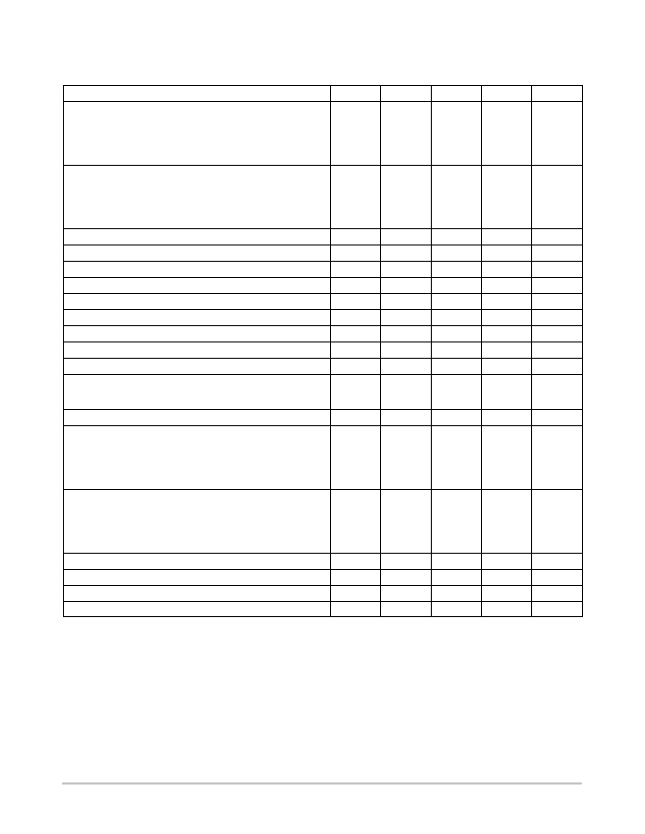
ELECTRICAL CHARACTERISTICS (Vin = Vout(nom) + 1.0 V, VCE = Vin, Cin = 2.2 mF, Cout = 2.2 mF, TA = 25°C,
unless otherwise noted)
Characteristic
Symbol
Min
Typ
Max
Unit
Output Voltage (TA = 25°C, Iout = 10 mA)
0.8 V
1.0 V
1.2 V
2.5 V
3.3 V
Vout
V
0.785
0.8
0.815
0.985
1.0
1.015
1.185
1.2
1.215
2.475
2.5
2.525
3.267
3.3
3.333
Output Voltage (TA = − 40°C to 85°C, Iout = 10 mA)
0.8 V
1.0 V
1.2 V
2.5 V
3.3 V
Vout
V
0.760
0.8
0.827
0.960
1.0
1.027
1.160
1.2
1.227
2.435
2.5
2.545
3.214
3.3
3.359
Output Current
Input Voltage
Line Regulation (Vin = Vout + 1.0 V to 6.5 V, Iout = 10 mA)
Load Regulation (Iout = 1 mA to 300 mA, Vin = Vout + 2.0 V)
Load Regulation (Iout = 1 mA to 1 A, Vin = Vout + 2.0 V)
Supply Current (Iout = 0 A, Vin = 6.5 V)
Standby Current (VCE = 0 V, Vin = 6.5 V)
Short Current Limit (Vout = 0 V)
Output Voltage Temperature Coefficient
Enable Input Threshold Voltage
(Voltage Increasing, Output Turns On, Logic High)
(Voltage Decreasing, Output Turns Off, Logic Low)
Iout
Vin
1.6
Regline
−
Regload03
−
Regload1
−
Iss
Istby
Ish
Tc
−
VthCE
1.0
−
1
0.05
20
80
65
0.15
250
$100
−
−
A
6.5
V
0.1
%/V
40
mV
120
mV
90
mA
0.6
mA
mA
−
ppm/°C
V
−
0.4
Enable Pulldown Current
0.3
mA
Drop Output Voltage (TA = 25°C, Iout = 300 mA)
0.8 V
1.0 V
1.2 V
2.5 V
3.3 V
Vin−Vout
V
0.670
0.780
0.450
0.610
0.300
0.500
0.150
0.310
0.130
0.170
Drop Output Voltage (TA = 25°C, Iout = 1 A)
0.8 V
1.0 V
1.2 V
2.5 V
3.3 V
Vin−Vout
V
1.150
1.650
1.000
1.450
0.870
1.380
0.500
1.100
0.430
0.650
Ripple Rejection (Ripple 200 mVpp, Iout = 100 mA, f = 1 kHz)
PSRR
70
dB
Output Noise (BW = 10 Hz to 100 kHz, Iout = 1 mA)
Vnoise
45
mVrms
Thermal Shutdown Temperature/Hysteresis
Tshd/Hyst
165/30
°C
RDS(on) of additional output transistor (D version only)
RDS(on)
30
W
2. Maximum package power dissipation limits must be observed.
3. Low duty cycle pulse techniques are used during testing to maintain the junction temperature as close to ambient as possible.
http://onsemi.com
3
Share Link: 