NCP1380 데이터 시트보기 (PDF) - ON Semiconductor
부품명
상세내역
일치하는 목록
NCP1380
ON Semiconductor

NCP1380 Datasheet PDF : 26 Pages
| |||
NCP1380
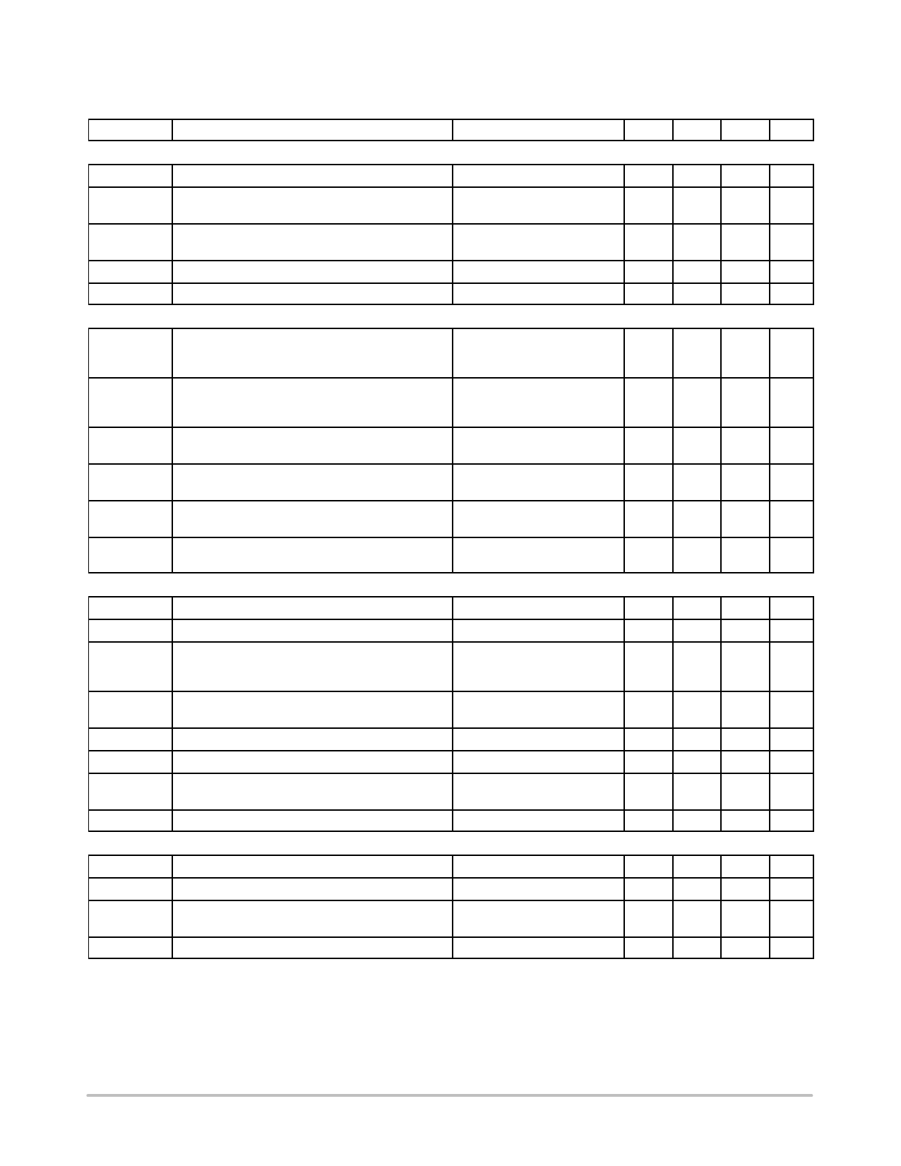
ELECTRICAL CHARACTERISTICS (Unless otherwise noted: For typical values TJ = 25°C, VCC = 12 V, VZCD = 0 V, VFB = 3 V,
VCS = 0 V, Vfault = 1.5 V, CT = 680 pF) For min/max values TJ = −40°C to +125°C, Max TJ = 150°C, VCC = 12 V)
Symbol
Condition
Min Typ Max Unit
CURRENT COMPARATOR − CURRENT SENSE
tILIM
Ipeak(VCO)
Propagation Delay
Percentage of maximum peak current level at
which VCO takes over (Note 4)
VCS > VILIM to DRV turn−off
−
125 175 ns
VFB = 0.4 V, VCS increasing
15.4 17.5 19.6
%
VOPP(MAX) Setpoint decrease for VZCD = −300 mV (Note 5)
VZCD = −300 mV, VFB = 4 V,
35
37.5
40
%
VCS increasing
VCS(stop)
Threshold for immediate fault protection activation
1.125 1.200 1.275 V
tBCS
Leading Edge Blanking Duration for VCS(stop)
−
120
−
ns
DRIVE OUTPUT − GATE DRIVE
RSNK
RSRC
ISNK
ISRC
tr
Drive Resistance
DRV Sink
DRV Source
Drive current capability
DRV Sink
DRV Source
Rise Time (10% to 90%)
VDRV = 10 V
VDRV = 2 V
W
−
12.5
−
−
20
−
VDRV = 10 V
VDRV = 2 V
mA
−
800
−
−
500
−
CDRV = 1 nF, VDRV from 0 to
−
12 V
40
75
ns
tf
Fall Time (90% to 10%)
CDRV = 1 nF, VDRV from 0 to
−
12 V
25
60
ns
VDRV(low)
DRV Low Voltage
VCC = VCC(off) + 0.2 V
8.4
9.1
−
V
CDRV = 1 nF, RDRV = 33 kW
VDRV(high) DRV High Voltage (Note 6)
VCC = VCC(MAX)
CDRV = 1 nF
10.5 13.0 15.5
V
DEMAGNETIZATION INPUT − ZERO VOLTAGE DETECTION CIRCUIT
VZCD(TH)
VZCD(HYS)
VCH
VCL
tDEM
ZCD threshold voltage
ZCD hysteresis
Input clamp voltage
High state
Low state
Propagation Delay
VZCD decreasing
35
55
90
mV
VZCD increasing
15
35
55
mV
Ipin1 = 3.0 mA
Ipin1 = −2.0 mA
V
8
10
12
−0.9 −0.7 −0.3
VZCD decreasing from 4 V to
−
−0.3 V
150 250 ns
CPAR
Internal input capacitance
tBLANK
Blanking delay after on−time
toutSS
tout
Timeout after last demag transition
RZCD(pdown) Pulldown resistor (Note 3)
TIMING CAPACITOR
During soft−start
After the end of soft−start
−
10
−
pF
2.30 3.15 4.00 ms
28
41
54
ms
5.0
5.9
6.7
140 320 500 kW
VCT(MAX)
ICT
VCT(MIN)
Maximum voltage on CT pin
Source current
Minimum voltage on CT pin, discharge switch
activated
VFB < VFB(TH)
VCT = 0 V
5.15 5.40 5.65
V
18
20
22
mA
−
−
90
mV
CT
Recommended timing capacitor value
220
pF
3. Guaranteed by design.
4. The peak current setpoint goes down as the load decreases. It is frozen below Ipeak(VCO) (Ipeak = cst)
5. If negative voltage in excess to −300 mV is applied to ZCD pin, the current setpoint decrease is no longer guaranteed to be linear
6. Minimum value for TJ = 125°C
7. NTC with R110 = 8.8 kW.
http://onsemi.com
7
Share Link: