M38504M6-201FP 데이터 시트보기 (PDF) - MITSUBISHI ELECTRIC
부품명
상세내역
일치하는 목록
M38504M6-201FP Datasheet PDF : 52 Pages
| |||
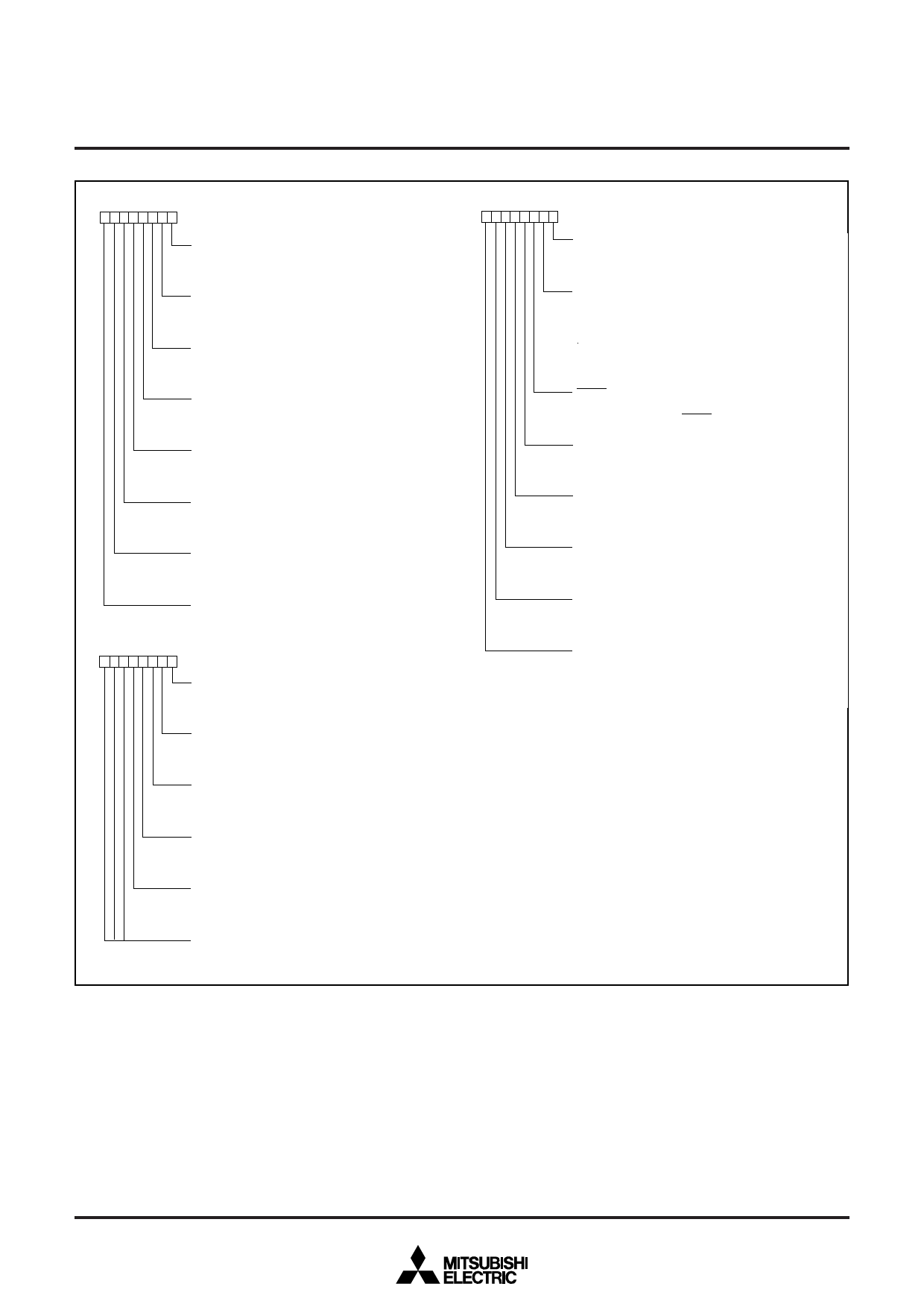
b7
b0 Serial I/O status register
(SIOSTS : address 0019 16)
Transmit buffer empty flag (TBE)
0: Buffer full
1: Buffer empty
Receive buffer full flag (RBF)
0: Buffer empty
1: Buffer full
Transmit shift completion flag (TSC)
0: Transmit shift in progress
1: Transmit shift completed
Overrun error flag (OE)
0: No error
1: Overrun error
Parity error flag (PE)
0: No error
1: Parity error
Framing error flag (FE)
0: No error
1: Framing error
Summing error flag (SE)
0: (OE) U (PE) U (FE)=0
1: (OE) U (PE) U (FE)=1
Not used (returns “1” when read)
b7
b0 UART control register
(UARTCON : address 001B 16)
Character length selection bit (CHAS)
0: 8 bits
1: 7 bits
Parity enable bit (PARE)
0: Parity checking disabled
1: Parity checking enabled
Parity selection bit (PARS)
0: Even parity
1: Odd parity
Stop bit length selection bit (STPS)
0: 1 stop bit
1: 2 stop bits
P25/TXD P-channel output disable bit (POFF)
0: CMOS output (in output mode)
1: N-channel open drain output (in output mode)
Not used (return “1” when read)
Fig. 19 Structure of serial I/O control registers
MITSUBISHI MICROCOMPUTERS
3850 Group
SINGLE-CHIP 8-BIT CMOS MICROCOMPUTER
b7
b0
Serial I/O control register
(SIOCON : address 001A 16)
BRG count source selection bit (CSS)
0: f(XIN)
1: f(XIN)/4
Serial I/O synchronous clock selection bit (SCS)
0: BRG output divided by 4 when clock synchronous
serial I/O is selected, BRG output divided by 16
when UART is selected.
1: External clock input when clock synchronous serial
I/O is selected, external clock input divided by 16
when UART is selected.
SRDY output enable bit (SRDY)
0: P27 pin operates as ordinary I/O pin
1: P27 pin operates as S RDY output pin
Transmit interrupt source selection bit (TIC)
0: Interrupt when transmit buffer has emptied
1: Interrupt when transmit shift operation is completed
Transmit enable bit (TE)
0: Transmit disabled
1: Transmit enabled
Receive enable bit (RE)
0: Receive disabled
1: Receive enabled
Serial I/O mode selection bit (SIOM)
0: Clock asynchronous (UART) serial I/O
1: Clock synchronous serial I/O
Serial I/O enable bit (SIOE)
0: Serial I/O disabled
(pins P24 to P27 operate as ordinary I/O pins)
1: Serial I/O enabled
(pins P24 to P27 operate as serial I/O pins)
20
Share Link: 