M37640E8FP 데이터 시트보기 (PDF) - Mitsumi
부품명
상세내역
일치하는 목록
M37640E8FP Datasheet PDF : 96 Pages
| |||
Ver 1.4
MITSUBISHI MICROCOMPUTERS
7640 Group
SINGLE-CHIP 8-BIT CMOS MICROCOMPUTER
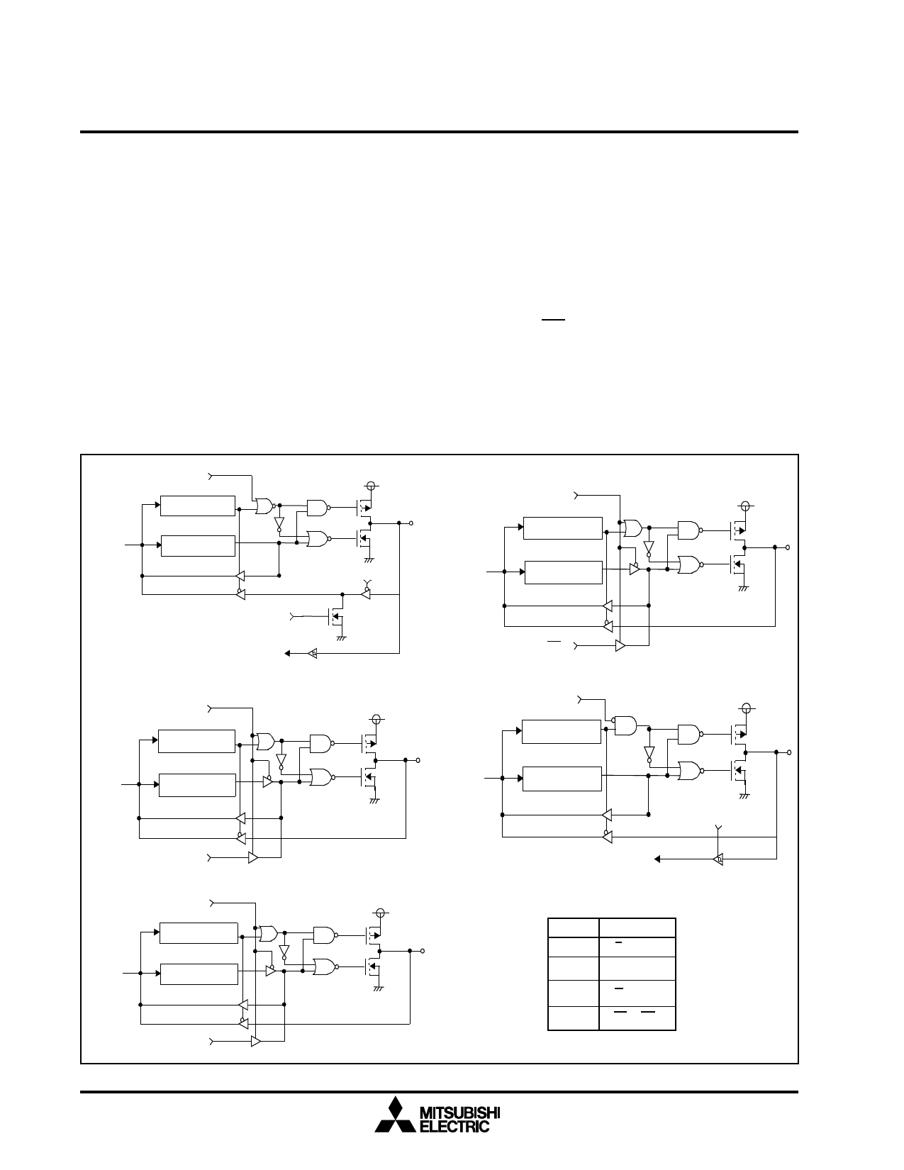
1.14.1.4 Port P5
Port 5 is an 8-bit general purpose I/O port that can be
configured to access special second functions. The
port can be set up in any configuration in all three pro-
cessor modes.
Port P50
This pin is multiplexed with the XCin clock input.
When the XCin clock is activated, the pin’s I/O is dis-
abled.
Port P51
This pin is multiplexed with the XCout clock output
and the Timer 1/2 pulse output. When the XCin clock
is activated, the pin’s I/O is disabled. If XCin is not be-
ing used as a system clock or XCout oscillation is dis-
abled, the pin can be configured as the Timer 1/2
pulse output pin. This feature is configured in the
Timer123 mode register as described in section 1.17.
Port P52- P57
These pins are multiplexed with control pins for the
bus interface control block. P52 acts as OBF0 output
to a Master CPU when DBBC00 is “1”.
P53 acts as IBF0 output to a Master CPU when
DBBC01 is “1”.
P54-P57 act as input control signals from a Master
CPU when DBBC06 is “1”. The table featured in Fig-
ure 1.17 shows the bus interface control signal that
corresponds to each pin.
Port P50
CPMA4
Direction Register
Data Bus
Port Latch
CPMA4
Port P53
DBBC01
Direction Register
Data Bus
Port Latch
CPMA4
Port P51
Tout Enable Bit
Direction Register
XCin Input
Data Bus
Port Latch
Port 52
Timer 1/2 Output
DBBC00
Direction Register
Data Bus
Port Latch
OBF0
Fig. 1.17. Port P5 Block Diagram
20
IBF0
Port P54 - P57
DBBC06
Direction Register
Data Bus
Port Latch
DBBC06
Port 54 - P57 Function
see table
for function
Pin
Function
P54
S0
P55
A0
P56
R(E)
P57
W(R/W)
Share Link: 