M37640E8FP 데이터 시트보기 (PDF) - Mitsumi
부품명
상세내역
일치하는 목록
M37640E8FP Datasheet PDF : 96 Pages
| |||
Ver 1.4
MITSUBISHI MICROCOMPUTERS
7640 Group
SINGLE-CHIP 8-BIT CMOS MICROCOMPUTER
1.14.1 I/O Ports
This device has 66 programmable I/O pins arranged
as ports P00 to P87. Each port bit can be configured
as input or output. To set the I/O port bit direction,
write a “1” to the corresponding direction register bit
to select output mode, or write a “0” to the direction
register bit to select input mode.
At reset, all of the direction registers are initialized to
0016, setting all of the I/O ports to input mode.
If data is written to a pin and then read from that pin
while it is in output mode, the data read is the value of
the port latch rather than the value of the pin itself.
Therefore, if an external load changes the value of an
output pin, the intended output value will still be read
correctly. Pins set to input mode are floating (pro-
vided that the pull up resistors are not being used) to
ensure that the value input to such a pin can be read
accurately. In the case when data is written to a pin
configured as an input, the data is written only to the
port latch; the pin itself remains floating.
Most of the I/O Ports are multiplexed with secondary
functions. When a GPI/O is multiplexed with a sec-
ond function, the control signal from the peripheral
overrides the direction register. The multiplexing is
briefly described below. The second function signals
to and from the I/O ports are described in detail in
their respective block’s description.
1.14.1.1 Ports P0, P1, and P3
Ports P0 and P1 act as the address bus (AB0-AB15)
in Microprocessor and Memory Expansion modes.
Bits 0 and 3-7 of Port P3 acts as control signals in
Microprocessor and Memory Expansion modes.
1.14.1.2 Port P2
Port P2 is an 8-bit general purpose I/O port when in
single chip mode. In this mode, the port has key-on
wake up circuitry which can be used to restart the
chip externally from a WIT or STP low power mode.
This port also acts as the data bus during micropro-
cessor and memory expansion modes. Port P2 input
level can be set to reduced VIHL level or CMOS level
by bit 6 of the port control register (PTC).
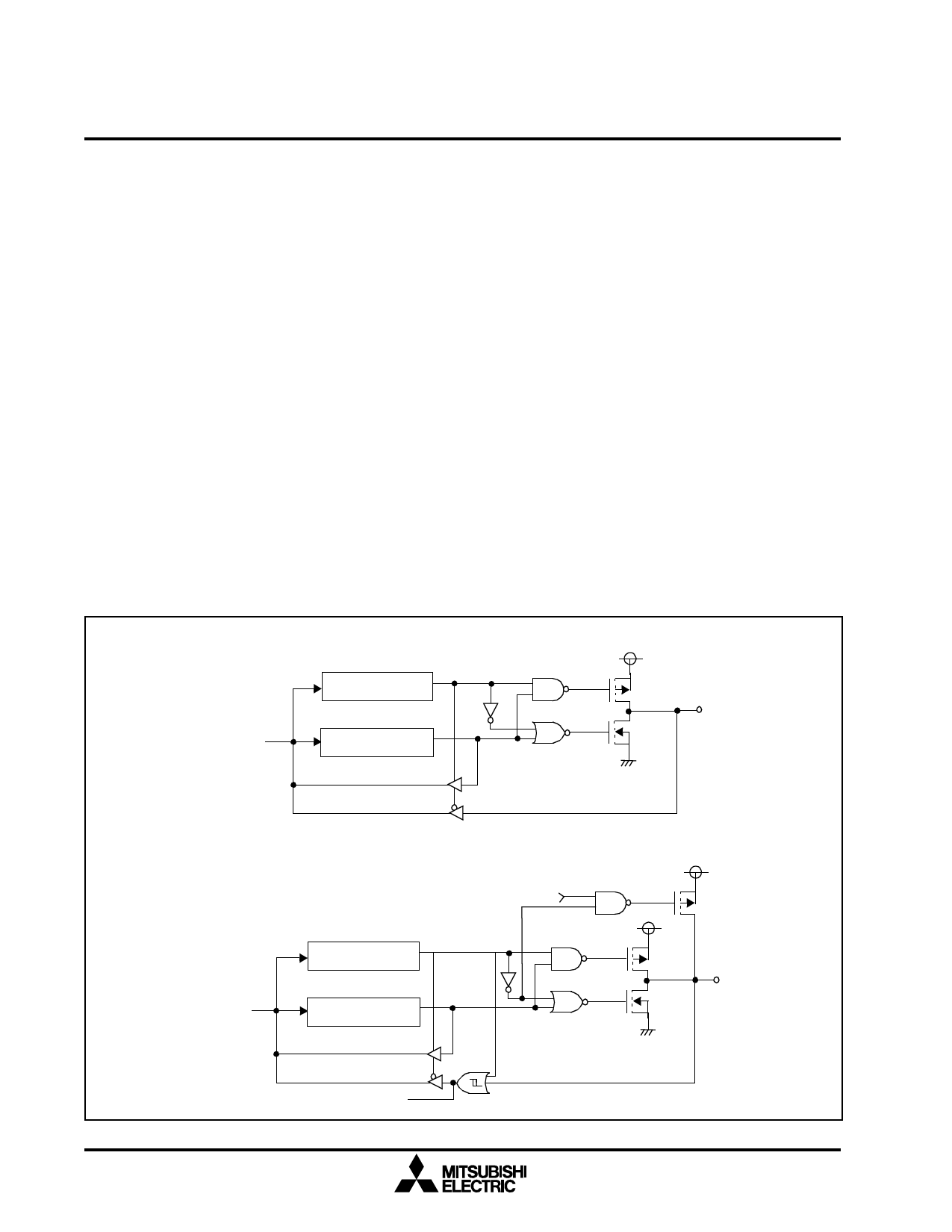
Ports P0, P1, P3
Direction Register
Data Bus
Port Latch
Port P2
Data Bus
Direction Register
Port Latch
Pull-up Control
Key-on Wake up Input
Fig. 1.15. Ports P0, P1, P2, P3 Block Diagram
18
Share Link: 